D at a S h e e t , D S 2 .1 , J u l y 2 00 3
DELIC-LC
DELIC-PB
DSP Embedded Line and
Port Interface Controller
PEB 20570 Version 3.1
PEB 20571 Version 3.1
Wire d
Communications
N e v e r
s t o p
t h i n k i n g .
�Edition 2003-07-31
Published by Infineon Technologies AG,
St.-Martin-Strasse 53,
D-81541 München, Germany
© Infineon Technologies AG 8/4/03.
All Rights Reserved.
Attention please!
The information herein is given to describe certain components and shall not be considered as warranted
characteristics.
Terms of delivery and rights to technical change reserved.
We hereby disclaim any and all warranties, including but not limited to warranties of non-infringement, regarding
circuits, descriptions and charts stated herein.
Infineon Technologies is an approved CECC manufacturer.
Information
For further information on technology, delivery terms and conditions and prices please contact your nearest
Infineon Technologies Office in Germany or our Infineon Technologies Representatives worldwide (see address
list).
Warnings
Due to technical requirements components may contain dangerous substances. For information on the types in
question please contact your nearest Infineon Technologies Office.
Infineon Technologies Components may only be used in life-support devices or systems with the express written
approval of Infineon Technologies, if a failure of such components can reasonably be expected to cause the failure
of that life-support device or system, or to affect the safety or effectiveness of that device or system. Life support
devices or systems are intended to be implanted in the human body, or to support and/or maintain and sustain
and/or protect human life. If they fail, it is reasonable to assume that the health of the user or other persons may
be endangered.
�D at a S h e e t , D S 2 .1 , J u l y 2 00 3
DELIC-LC
DELIC-PB
DSP Embedded Line and
Port Interface Controller
PEB 20570 Version 3.1
PEB 20571 Version 3.1
Wire d
Communications
N e v e r
s t o p
t h i n k i n g .
�PEB 20570
Revision History:
2003-07-31
Previous Version:
DS2
Page
DS 2.1
Subjects (major changes since last revision)
Trademarks updated
For questions on technology, delivery and prices please contact the Infineon
Technologies Offices in Germany or the Infineon Technologies Companies and
Representatives worldwide: see our webpage at http://www.infineon.com
Note: OCEM® and OakDSPCore® (OAK®) are registered trademarks of ParthusCeva,
Inc..
�PEB 20570
PEB 20571
Table of Contents
Page
1
1.1
1.2
1.3
1.4
1.4.1
1.4.2
Introduction . . . . . . . . . . . . . . . . . . . . . . . . . . . . . . . . . . . . . . . . . . . . . . . .
DELIC-LC Key Features . . . . . . . . . . . . . . . . . . . . . . . . . . . . . . . . . . . . . . .
DELIC-PB Key Features . . . . . . . . . . . . . . . . . . . . . . . . . . . . . . . . . . . . . . .
Logic Symbol . . . . . . . . . . . . . . . . . . . . . . . . . . . . . . . . . . . . . . . . . . . . . . . .
Typical Applications . . . . . . . . . . . . . . . . . . . . . . . . . . . . . . . . . . . . . . . . . . .
Applications for DELIC-LC . . . . . . . . . . . . . . . . . . . . . . . . . . . . . . . . . . . .
Applications for DELIC-PB . . . . . . . . . . . . . . . . . . . . . . . . . . . . . . . . . . . .
2
4
4
6
7
7
8
2
2.1
2.2
2.3
2.4
2.5
Pin Description . . . . . . . . . . . . . . . . . . . . . . . . . . . . . . . . . . . . . . . . . . . .
Pin Diagram DELIC-LC . . . . . . . . . . . . . . . . . . . . . . . . . . . . . . . . . . . . . . .
Pin Diagram DELIC-PB . . . . . . . . . . . . . . . . . . . . . . . . . . . . . . . . . . . . . . .
Pin Definitions and Functions for DELIC-LC . . . . . . . . . . . . . . . . . . . . . . .
Pin Definitions and Functions for DELIC-PB . . . . . . . . . . . . . . . . . . . . . . .
Strap Pin Definitions . . . . . . . . . . . . . . . . . . . . . . . . . . . . . . . . . . . . . . . . .
10
10
11
12
24
38
3
3.1
3.2
3.2.1
3.2.2
3.2.2.1
3.2.2.2
3.2.3
3.2.3.1
3.2.3.2
3.2.4
3.2.4.1
3.2.4.2
3.3
3.3.1
3.4
3.4.1
3.4.2
3.4.3
3.4.4
3.5
3.5.1
3.5.2
Interface Description . . . . . . . . . . . . . . . . . . . . . . . . . . . . . . . . . . . . . . . .
Overview of Interfaces . . . . . . . . . . . . . . . . . . . . . . . . . . . . . . . . . . . . . . . .
IOM-2000 Interface . . . . . . . . . . . . . . . . . . . . . . . . . . . . . . . . . . . . . . . . . .
Overview . . . . . . . . . . . . . . . . . . . . . . . . . . . . . . . . . . . . . . . . . . . . . . . .
IOM-2000 Frame Structure . . . . . . . . . . . . . . . . . . . . . . . . . . . . . . . . . .
Data Interface . . . . . . . . . . . . . . . . . . . . . . . . . . . . . . . . . . . . . . . . . .
Command and Status Interface . . . . . . . . . . . . . . . . . . . . . . . . . . . . .
UPN State Machine . . . . . . . . . . . . . . . . . . . . . . . . . . . . . . . . . . . . . . . .
INFO Structure on the UPN Interface . . . . . . . . . . . . . . . . . . . . . . . .
UPN Mode State Diagram . . . . . . . . . . . . . . . . . . . . . . . . . . . . . . . . .
S/T State Machine . . . . . . . . . . . . . . . . . . . . . . . . . . . . . . . . . . . . . . . . .
LT-S Mode . . . . . . . . . . . . . . . . . . . . . . . . . . . . . . . . . . . . . . . . . . . . .
LT-T Mode . . . . . . . . . . . . . . . . . . . . . . . . . . . . . . . . . . . . . . . . . . . . .
IOM®-2 Interface . . . . . . . . . . . . . . . . . . . . . . . . . . . . . . . . . . . . . . . . . . . .
Signals / Channels . . . . . . . . . . . . . . . . . . . . . . . . . . . . . . . . . . . . . . . . .
µP Interface . . . . . . . . . . . . . . . . . . . . . . . . . . . . . . . . . . . . . . . . . . . . . . . .
Intel/Infineon or Motorola Mode . . . . . . . . . . . . . . . . . . . . . . . . . . . . . . .
De-Multiplexed or Multiplexed Mode . . . . . . . . . . . . . . . . . . . . . . . . . . .
DMA or Non-DMA Mode . . . . . . . . . . . . . . . . . . . . . . . . . . . . . . . . . . . .
DELIC External Interrupts . . . . . . . . . . . . . . . . . . . . . . . . . . . . . . . . . . .
JTAG Test Interface . . . . . . . . . . . . . . . . . . . . . . . . . . . . . . . . . . . . . . . . . .
Boundary Scan Test . . . . . . . . . . . . . . . . . . . . . . . . . . . . . . . . . . . . . . .
TAP Controller . . . . . . . . . . . . . . . . . . . . . . . . . . . . . . . . . . . . . . . . . . . .
40
40
41
41
42
42
45
48
48
50
54
55
58
63
63
64
64
64
66
66
67
67
67
4
4.1
4.2
4.2.1
4.2.2
Functional Description . . . . . . . . . . . . . . . . . . . . . . . . . . . . . . . . . . . . . .
Functional Overview and Block Diagram . . . . . . . . . . . . . . . . . . . . . . . . . .
IOM-2000 Transceiver Unit (TRANSIU) . . . . . . . . . . . . . . . . . . . . . . . . . .
IOM-2000 Features . . . . . . . . . . . . . . . . . . . . . . . . . . . . . . . . . . . . . . . .
IOM-2000 Initialization . . . . . . . . . . . . . . . . . . . . . . . . . . . . . . . . . . . . . .
69
70
71
71
71
Data Sheet
2003-07-31
�PEB 20570
PEB 20571
Table of Contents
Page
4.2.3
Initialization of the VIP . . . . . . . . . . . . . . . . . . . . . . . . . . . . . . . . . . . . . . 72
4.2.4
IOM-2000 Command and Status Interface . . . . . . . . . . . . . . . . . . . . . . 72
4.2.4.1
Initialization Mode Command Bits . . . . . . . . . . . . . . . . . . . . . . . . . . . 72
4.2.4.2
Operational Mode Command/Status Bits . . . . . . . . . . . . . . . . . . . . . 72
4.2.4.3
Command/Status Transmission . . . . . . . . . . . . . . . . . . . . . . . . . . . . . 72
4.2.4.4
Command and Status format in the Data RAM . . . . . . . . . . . . . . . . . 74
4.2.5
UPN Mode Frame Structure . . . . . . . . . . . . . . . . . . . . . . . . . . . . . . . . . 76
4.2.6
UPN Interface . . . . . . . . . . . . . . . . . . . . . . . . . . . . . . . . . . . . . . . . . . . . 79
4.2.7
UPN Framing Bit Description . . . . . . . . . . . . . . . . . . . . . . . . . . . . . . . . . 80
4.2.7.1
Framing Bit (LF-Bit) . . . . . . . . . . . . . . . . . . . . . . . . . . . . . . . . . . . . . . 80
4.2.7.2
Multiframing Bit (M-Bit) . . . . . . . . . . . . . . . . . . . . . . . . . . . . . . . . . . . 80
4.2.7.3
DC-Balancing Bit . . . . . . . . . . . . . . . . . . . . . . . . . . . . . . . . . . . . . . . . 81
4.2.7.4
UPN Mode Data Format . . . . . . . . . . . . . . . . . . . . . . . . . . . . . . . . . . 81
4.2.7.5
UPN Scrambler/Descrambler . . . . . . . . . . . . . . . . . . . . . . . . . . . . . . 82
4.2.8
DECT Synchronization for UPN- Interface . . . . . . . . . . . . . . . . . . . . . . 82
4.2.9
S/T Interface Frame Structure . . . . . . . . . . . . . . . . . . . . . . . . . . . . . . . . 83
4.2.9.1
LT-S mode . . . . . . . . . . . . . . . . . . . . . . . . . . . . . . . . . . . . . . . . . . . . . 86
4.2.9.2
LT-T Mode . . . . . . . . . . . . . . . . . . . . . . . . . . . . . . . . . . . . . . . . . . . . . 88
4.2.10
S/T Mode Control and Framing Bits on IOM-2000 . . . . . . . . . . . . . . . . 90
4.2.10.1
Framing Bit (F-Bit) . . . . . . . . . . . . . . . . . . . . . . . . . . . . . . . . . . . . . . . 90
4.2.10.2
Multiframing Bits . . . . . . . . . . . . . . . . . . . . . . . . . . . . . . . . . . . . . . . . 90
4.2.10.3
Fa/N Bit . . . . . . . . . . . . . . . . . . . . . . . . . . . . . . . . . . . . . . . . . . . . . . . 92
4.2.10.4
DC-Balancing Bit (L-Bit) . . . . . . . . . . . . . . . . . . . . . . . . . . . . . . . . . . . 93
4.2.11
IOM-2000 Data Interface . . . . . . . . . . . . . . . . . . . . . . . . . . . . . . . . . . . . 93
4.2.11.1
S/T Mode Data Format . . . . . . . . . . . . . . . . . . . . . . . . . . . . . . . . . . . 93
4.2.12
Test Loop . . . . . . . . . . . . . . . . . . . . . . . . . . . . . . . . . . . . . . . . . . . . . . . . 94
4.3
IOM-2 Unit . . . . . . . . . . . . . . . . . . . . . . . . . . . . . . . . . . . . . . . . . . . . . . . . . 95
4.3.1
IOMU Features . . . . . . . . . . . . . . . . . . . . . . . . . . . . . . . . . . . . . . . . . . . 95
4.3.2
IOMU Functional and Operational Description . . . . . . . . . . . . . . . . . . . 96
4.3.2.1
Frame-Wise Buffer Swapping . . . . . . . . . . . . . . . . . . . . . . . . . . . . . . 96
4.3.2.2
DSP Inaccessible Buffer (I-buffer) Logical Structure . . . . . . . . . . . . . 96
4.3.2.3
DSP Access to the D-Buffer . . . . . . . . . . . . . . . . . . . . . . . . . . . . . . . 97
4.3.2.4
Circular Buffer Architecture . . . . . . . . . . . . . . . . . . . . . . . . . . . . . . . . 98
4.3.2.5
IOM-2 Interface Data Rate Modes . . . . . . . . . . . . . . . . . . . . . . . . . . 100
4.3.2.6
IOMU Serial Data Processing . . . . . . . . . . . . . . . . . . . . . . . . . . . . . 101
4.3.2.7
IOMU Parallel Data Processing . . . . . . . . . . . . . . . . . . . . . . . . . . . . 101
4.3.2.8
IOM-2 Push-Pull and Open-Drain Modes . . . . . . . . . . . . . . . . . . . . 102
4.3.2.9
Support of DRDY Signal from QUAT-S . . . . . . . . . . . . . . . . . . . . . . 103
4.4
PCM Unit . . . . . . . . . . . . . . . . . . . . . . . . . . . . . . . . . . . . . . . . . . . . . . . . . 104
4.4.1
PCMU Functional and Operational Description . . . . . . . . . . . . . . . . . . 105
4.4.1.1
Frame-Wise Buffer Swapping . . . . . . . . . . . . . . . . . . . . . . . . . . . . . 105
4.4.1.2
DSP Inaccessible Buffer (I-buffer) . . . . . . . . . . . . . . . . . . . . . . . . . . 105
Data Sheet
2003-07-31
�PEB 20570
PEB 20571
Table of Contents
4.4.1.3
4.4.1.4
4.4.1.5
4.4.1.6
4.4.1.7
4.5
4.6
4.6.1
4.6.2
4.6.2.1
4.6.2.2
4.6.2.3
4.6.2.4
4.6.2.5
4.6.3
4.7
4.7.1
4.7.2
4.7.3
4.7.3.1
4.7.3.2
4.7.4
4.7.5
4.7.6
4.7.6.1
4.7.7
4.7.8
4.7.9
4.8
4.8.1
4.8.2
4.8.3
4.8.4
4.8.5
4.8.6
4.8.7
4.9
4.9.1
4.9.2
4.9.3
4.10
4.10.1
Data Sheet
Page
DSP Accessible Buffer (D-Buffer) . . . . . . . . . . . . . . . . . . . . . . . . . .
PCMU Interface Data Rate Modes . . . . . . . . . . . . . . . . . . . . . . . . .
PCMU Serial Data Processing . . . . . . . . . . . . . . . . . . . . . . . . . . . . .
PCMU Parallel Data Processing . . . . . . . . . . . . . . . . . . . . . . . . . . .
PCMU Tri-state Control Logic . . . . . . . . . . . . . . . . . . . . . . . . . . . . .
A-/µ-law Conversion Unit . . . . . . . . . . . . . . . . . . . . . . . . . . . . . . . . . . . . .
HDLC Unit . . . . . . . . . . . . . . . . . . . . . . . . . . . . . . . . . . . . . . . . . . . . . . . .
HDLC Overview . . . . . . . . . . . . . . . . . . . . . . . . . . . . . . . . . . . . . . . . . .
HDLCU Operation . . . . . . . . . . . . . . . . . . . . . . . . . . . . . . . . . . . . . . . .
Initialization of the HDLCU . . . . . . . . . . . . . . . . . . . . . . . . . . . . . . . .
Transmitting a Message . . . . . . . . . . . . . . . . . . . . . . . . . . . . . . . . .
Ending a Transmission . . . . . . . . . . . . . . . . . . . . . . . . . . . . . . . . . .
Aborting a Transmission . . . . . . . . . . . . . . . . . . . . . . . . . . . . . . . . .
DSP Access to the HDLCU Buffers . . . . . . . . . . . . . . . . . . . . . . . . .
Functionality . . . . . . . . . . . . . . . . . . . . . . . . . . . . . . . . . . . . . . . . . . . . .
GHDLC Unit . . . . . . . . . . . . . . . . . . . . . . . . . . . . . . . . . . . . . . . . . . . . . . .
GHDLC Overview . . . . . . . . . . . . . . . . . . . . . . . . . . . . . . . . . . . . . . . .
GHDLC General Modes of Operation . . . . . . . . . . . . . . . . . . . . . . . . .
External Configuration and Handshaking in Bus Mode . . . . . . . . . . . .
External Tri-State in Point-to-Multi-Point Mode . . . . . . . . . . . . . . . .
Arbitration Between Several GHDLCs . . . . . . . . . . . . . . . . . . . . . . .
GHDLC Memory Allocation . . . . . . . . . . . . . . . . . . . . . . . . . . . . . . . . .
GHDLC Interrupts . . . . . . . . . . . . . . . . . . . . . . . . . . . . . . . . . . . . . . . .
Operational Description . . . . . . . . . . . . . . . . . . . . . . . . . . . . . . . . . . . .
GHDLC Initialization . . . . . . . . . . . . . . . . . . . . . . . . . . . . . . . . . . . .
GHDLC Protocol Features . . . . . . . . . . . . . . . . . . . . . . . . . . . . . . . . . .
GHDLC possible Data Rates for the DELIC-LC/PB . . . . . . . . . . . . . . .
GHDLC Using external DMA Controller . . . . . . . . . . . . . . . . . . . . . . . .
DSP Control Unit . . . . . . . . . . . . . . . . . . . . . . . . . . . . . . . . . . . . . . . . . . .
General . . . . . . . . . . . . . . . . . . . . . . . . . . . . . . . . . . . . . . . . . . . . . . . .
DSP Address Decoding . . . . . . . . . . . . . . . . . . . . . . . . . . . . . . . . . . . .
Interrupt Handling . . . . . . . . . . . . . . . . . . . . . . . . . . . . . . . . . . . . . . . .
DSP Run Time Statistics . . . . . . . . . . . . . . . . . . . . . . . . . . . . . . . . . . .
Data Bus and Program Bus Arbitration . . . . . . . . . . . . . . . . . . . . . . . .
Boot Support . . . . . . . . . . . . . . . . . . . . . . . . . . . . . . . . . . . . . . . . . . . .
Reset Execution and Boot Strap Pin Setting . . . . . . . . . . . . . . . . . . . .
General Mailbox . . . . . . . . . . . . . . . . . . . . . . . . . . . . . . . . . . . . . . . . . . . .
Overview . . . . . . . . . . . . . . . . . . . . . . . . . . . . . . . . . . . . . . . . . . . . . . .
µP Mailbox . . . . . . . . . . . . . . . . . . . . . . . . . . . . . . . . . . . . . . . . . . . . . .
OAK Mailbox . . . . . . . . . . . . . . . . . . . . . . . . . . . . . . . . . . . . . . . . . . . .
DMA Mailbox (DELIC-PB only). . . . . . . . . . . . . . . . . . . . . . . . . . . . . . . . .
DMA Handshake . . . . . . . . . . . . . . . . . . . . . . . . . . . . . . . . . . . . . . . . .
106
107
108
108
109
111
113
113
115
115
115
116
116
116
116
119
119
119
120
120
120
122
124
124
124
125
125
126
127
127
127
127
128
129
129
130
131
131
131
132
133
136
2003-07-31
�PEB 20570
PEB 20571
Table of Contents
Page
4.10.1.1
Two-cycle DMA Transfer Mode . . . . . . . . . . . . . . . . . . . . . . . . . . . .
4.10.1.2
Fly-by Mode . . . . . . . . . . . . . . . . . . . . . . . . . . . . . . . . . . . . . . . . . . .
4.10.2
PEC Mode. . . . . . . . . . . . . . . . . . . . . . . . . . . . . . . . . . . . . . . . . . . . . .
4.10.3
Transmit DMA Mailbox . . . . . . . . . . . . . . . . . . . . . . . . . . . . . . . . . . . .
4.10.4
Receive DMA Mailbox . . . . . . . . . . . . . . . . . . . . . . . . . . . . . . . . . . . . .
4.10.5
FIFO Access . . . . . . . . . . . . . . . . . . . . . . . . . . . . . . . . . . . . . . . . . . . .
4.11
Clock Generator . . . . . . . . . . . . . . . . . . . . . . . . . . . . . . . . . . . . . . . . . . . .
4.11.1
Overview . . . . . . . . . . . . . . . . . . . . . . . . . . . . . . . . . . . . . . . . . . . . . . .
4.11.2
DSP Clock Selection . . . . . . . . . . . . . . . . . . . . . . . . . . . . . . . . . . . . . .
4.11.3
PCM Master/Slave Mode Clocks Selection . . . . . . . . . . . . . . . . . . . . .
4.11.4
DELIC Clock System Synchronization . . . . . . . . . . . . . . . . . . . . . . . . .
4.11.5
IOM-2 Clock Selection . . . . . . . . . . . . . . . . . . . . . . . . . . . . . . . . . . . . .
4.11.6
IOM-2000 Clock Selection . . . . . . . . . . . . . . . . . . . . . . . . . . . . . . . . . .
4.11.7
REFCLK Configuration . . . . . . . . . . . . . . . . . . . . . . . . . . . . . . . . . . . .
4.11.8
GHDLC Clock Selection . . . . . . . . . . . . . . . . . . . . . . . . . . . . . . . . . . .
137
137
137
137
139
141
142
142
144
144
144
144
145
145
145
5
5.1
5.1.1
5.1.2
5.1.3
5.2
DELIC Memory Structure . . . . . . . . . . . . . . . . . . . . . . . . . . . . . . . . . . .
DSP Address Space . . . . . . . . . . . . . . . . . . . . . . . . . . . . . . . . . . . . . . . .
DSP Register Address Space . . . . . . . . . . . . . . . . . . . . . . . . . . . . . . .
DSP Program Address Space . . . . . . . . . . . . . . . . . . . . . . . . . . . . . . .
DSP Data Address Space . . . . . . . . . . . . . . . . . . . . . . . . . . . . . . . . . .
µP Address Space . . . . . . . . . . . . . . . . . . . . . . . . . . . . . . . . . . . . . . . . . .
146
146
146
146
147
150
6
6.1
6.2
6.2.1
6.2.1.1
6.2.1.2
6.2.1.3
6.2.1.4
6.2.1.5
6.2.1.6
6.2.1.7
6.2.1.8
6.2.1.9
6.2.2
6.2.2.1
6.2.2.2
6.2.2.3
6.2.2.4
6.2.2.5
6.2.3
Register Description . . . . . . . . . . . . . . . . . . . . . . . . . . . . . . . . . . . . . . .
Register Map . . . . . . . . . . . . . . . . . . . . . . . . . . . . . . . . . . . . . . . . . . . . . .
Detailed Register Description . . . . . . . . . . . . . . . . . . . . . . . . . . . . . . . . .
TRANSIU Register Description . . . . . . . . . . . . . . . . . . . . . . . . . . . . . .
TRANSIU IOM-2000 Configuration Register . . . . . . . . . . . . . . . . . .
TRANSIU Channel Configuration Registers . . . . . . . . . . . . . . . . . .
VIP Command Registers (VIPCMR0, VIPCMR1, VIPCMR2) . . . . .
VIP Status Registers . . . . . . . . . . . . . . . . . . . . . . . . . . . . . . . . . . . .
TRANSIU Initialization Channel Command Register . . . . . . . . . . . .
TRANSIU Initialization Channel Status Register (TICSTR) . . . . . . .
Up Test Loop Register . . . . . . . . . . . . . . . . . . . . . . . . . . . . . . . . . . .
Scrambler Mode Register . . . . . . . . . . . . . . . . . . . . . . . . . . . . . . . .
Scrambler Status Register . . . . . . . . . . . . . . . . . . . . . . . . . . . . . . . .
IOMU Register Description . . . . . . . . . . . . . . . . . . . . . . . . . . . . . . . . .
IOMU Control Register . . . . . . . . . . . . . . . . . . . . . . . . . . . . . . . . . .
IOMU Status Register . . . . . . . . . . . . . . . . . . . . . . . . . . . . . . . . . . .
IOMU Tri-State Control Register . . . . . . . . . . . . . . . . . . . . . . . . . . .
IOMU DRDY Register . . . . . . . . . . . . . . . . . . . . . . . . . . . . . . . . . . .
IOMU Data Prefix Register . . . . . . . . . . . . . . . . . . . . . . . . . . . . . . .
PCMU Register Description . . . . . . . . . . . . . . . . . . . . . . . . . . . . . . . . .
151
151
161
161
161
162
164
167
168
173
174
175
176
177
177
178
179
181
182
183
Data Sheet
2003-07-31
�PEB 20570
PEB 20571
Table of Contents
6.2.3.1
6.2.3.2
6.2.3.3
6.2.3.4
6.2.4
6.2.4.1
6.2.4.2
6.2.4.3
6.2.5
6.2.5.1
6.2.5.2
6.2.5.3
6.2.5.4
6.2.6
6.2.6.1
6.2.6.2
6.2.6.3
6.2.6.4
6.2.6.5
6.2.6.6
6.2.6.7
6.2.6.8
6.2.6.9
6.2.6.10
6.2.6.11
6.2.6.12
6.2.6.13
6.2.6.14
6.2.6.15
6.2.7
6.2.7.1
6.2.7.2
6.2.7.3
6.2.7.4
6.2.8
6.2.8.1
6.2.8.2
6.2.9
6.2.9.1
6.2.9.2
6.2.9.3
6.2.9.4
Data Sheet
Page
PCMU Command Register . . . . . . . . . . . . . . . . . . . . . . . . . . . . . . .
PCMU Status Register . . . . . . . . . . . . . . . . . . . . . . . . . . . . . . . . . . .
PCMU Tri-state Control Registers . . . . . . . . . . . . . . . . . . . . . . . . . .
PCMU Data Prefix Register . . . . . . . . . . . . . . . . . . . . . . . . . . . . . . .
A-/µ-law Unit Register Description . . . . . . . . . . . . . . . . . . . . . . . . . . . .
A/µ-law Unit Control Register . . . . . . . . . . . . . . . . . . . . . . . . . . . . .
A/µ-law Input Register . . . . . . . . . . . . . . . . . . . . . . . . . . . . . . . . . . .
A/µ-law Output Register . . . . . . . . . . . . . . . . . . . . . . . . . . . . . . . . . .
HDLCU Registers Description . . . . . . . . . . . . . . . . . . . . . . . . . . . . . . .
HDLCU Control Register . . . . . . . . . . . . . . . . . . . . . . . . . . . . . . . . .
HDLCU Status Register . . . . . . . . . . . . . . . . . . . . . . . . . . . . . . . . . .
Channel Command Vector . . . . . . . . . . . . . . . . . . . . . . . . . . . . . . .
Channel Status Vector . . . . . . . . . . . . . . . . . . . . . . . . . . . . . . . . . . .
GHDLC Register Description . . . . . . . . . . . . . . . . . . . . . . . . . . . . . . . .
GHDLC Test/ Normal Mode Register . . . . . . . . . . . . . . . . . . . . . . .
GHDLC Channel Mode Register . . . . . . . . . . . . . . . . . . . . . . . . . . .
GHDLC Interrupt Register . . . . . . . . . . . . . . . . . . . . . . . . . . . . . . . .
GHDLC FSC Interrupt Control Register . . . . . . . . . . . . . . . . . . . . . .
GHDLC Receive Channel Status Registers 0..3 . . . . . . . . . . . . . . .
GHDLC Receive Data and Status . . . . . . . . . . . . . . . . . . . . . . . . . .
GHDLC Mode Registers . . . . . . . . . . . . . . . . . . . . . . . . . . . . . . . . .
GHDLC Channel Transmit Command Registers . . . . . . . . . . . . . . .
ASYNC Control Register . . . . . . . . . . . . . . . . . . . . . . . . . . . . . . . . .
LCLK0 Control Register . . . . . . . . . . . . . . . . . . . . . . . . . . . . . . . . . .
LCLK1 Control Register . . . . . . . . . . . . . . . . . . . . . . . . . . . . . . . . . .
LCLK2 Control Register . . . . . . . . . . . . . . . . . . . . . . . . . . . . . . . . . .
LCLK3 Control Register . . . . . . . . . . . . . . . . . . . . . . . . . . . . . . . . . .
Muxes Control Register . . . . . . . . . . . . . . . . . . . . . . . . . . . . . . . . . .
GHDLCU Frame Frequency . . . . . . . . . . . . . . . . . . . . . . . . . . . . . .
DCU Register Description . . . . . . . . . . . . . . . . . . . . . . . . . . . . . . . . . .
Interrupt Mask Register . . . . . . . . . . . . . . . . . . . . . . . . . . . . . . . . . .
Status Event Register . . . . . . . . . . . . . . . . . . . . . . . . . . . . . . . . . . .
Statistics Counter Register . . . . . . . . . . . . . . . . . . . . . . . . . . . . . . .
Statistics Register . . . . . . . . . . . . . . . . . . . . . . . . . . . . . . . . . . . . . .
µP Configuration Registers . . . . . . . . . . . . . . . . . . . . . . . . . . . . . . . . .
µP Interface Configuration Register . . . . . . . . . . . . . . . . . . . . . . . . .
Interrupt Vector Register . . . . . . . . . . . . . . . . . . . . . . . . . . . . . . . . .
µP Mailbox Registers Description . . . . . . . . . . . . . . . . . . . . . . . . . . . .
µP Command Register . . . . . . . . . . . . . . . . . . . . . . . . . . . . . . . . . .
µP Mailbox Busy Register . . . . . . . . . . . . . . . . . . . . . . . . . . . . . . . .
µP Mailbox Generic Data Register . . . . . . . . . . . . . . . . . . . . . . . . .
µP Mailbox (General and DMA Mailbox) Data Registers . . . . . . . . .
183
184
185
187
188
188
189
190
191
191
192
193
195
197
197
198
199
200
201
203
204
206
207
208
209
210
211
212
213
214
214
215
216
217
218
218
220
221
221
222
223
224
2003-07-31
�PEB 20570
PEB 20571
Table of Contents
6.2.9.5
6.2.9.6
6.2.9.7
6.2.9.8
6.2.10
6.2.10.1
6.2.10.2
6.2.10.3
6.2.11
6.2.11.1
6.2.11.2
6.2.11.3
6.2.11.4
6.2.11.5
6.2.11.6
6.2.11.7
6.2.11.8
6.2.11.9
6.2.11.10
6.2.11.11
6.2.11.12
Page
DSP Command Register . . . . . . . . . . . . . . . . . . . . . . . . . . . . . . . . .
DSP Mailbox Busy Register . . . . . . . . . . . . . . . . . . . . . . . . . . . . . . .
DSP Mailbox Generic Data Register . . . . . . . . . . . . . . . . . . . . . . . .
DSP Mailbox (General and DMA Mailbox) Data Registers . . . . . . .
DMA Mailbox Registers Description . . . . . . . . . . . . . . . . . . . . . . . . . .
DMA Mailbox Transmit Counter Register . . . . . . . . . . . . . . . . . . . .
DMA Mailbox Receive Counter Register . . . . . . . . . . . . . . . . . . . . .
DMA Mailbox Interrupt Status Register . . . . . . . . . . . . . . . . . . . . . .
Clock Generator Register Description . . . . . . . . . . . . . . . . . . . . . . . . .
PDC Control Register . . . . . . . . . . . . . . . . . . . . . . . . . . . . . . . . . . .
PFS Control Register . . . . . . . . . . . . . . . . . . . . . . . . . . . . . . . . . . . .
CLKOUT Control Register . . . . . . . . . . . . . . . . . . . . . . . . . . . . . . . .
DCXO Reference Clock Select Register . . . . . . . . . . . . . . . . . . . . .
REFCLK Control Register . . . . . . . . . . . . . . . . . . . . . . . . . . . . . . . .
DCL_2000 Control Register . . . . . . . . . . . . . . . . . . . . . . . . . . . . . . .
DCL Control Register . . . . . . . . . . . . . . . . . . . . . . . . . . . . . . . . . . . .
FSC Control Register . . . . . . . . . . . . . . . . . . . . . . . . . . . . . . . . . . . .
L1_CLK Control Register . . . . . . . . . . . . . . . . . . . . . . . . . . . . . . . . .
PFS Sync Register . . . . . . . . . . . . . . . . . . . . . . . . . . . . . . . . . . . . .
Real-time Counter Register . . . . . . . . . . . . . . . . . . . . . . . . . . . . . . .
Strap Status Register . . . . . . . . . . . . . . . . . . . . . . . . . . . . . . . . . . . .
225
226
227
228
229
229
230
231
232
232
233
234
235
236
237
238
239
240
241
242
243
7
Package Outlines . . . . . . . . . . . . . . . . . . . . . . . . . . . . . . . . . . . . . . . . . . 244
8
8.1
8.2
8.3
8.4
8.5
8.6
8.6.1
8.6.1.1
8.6.1.2
8.6.2
8.6.2.1
8.6.2.2
8.6.3
8.6.4
8.6.5
8.6.6
8.6.7
8.6.8
Electrical Characteristics and Timing Diagrams . . . . . . . . . . . . . . . .
Absolute Maximum Ratings . . . . . . . . . . . . . . . . . . . . . . . . . . . . . . . . . . .
Operating Range . . . . . . . . . . . . . . . . . . . . . . . . . . . . . . . . . . . . . . . . . . .
DC Characteristics . . . . . . . . . . . . . . . . . . . . . . . . . . . . . . . . . . . . . . . . . .
Capacitances . . . . . . . . . . . . . . . . . . . . . . . . . . . . . . . . . . . . . . . . . . . . . .
Recommended 16.384 MHz Crystal Parameters . . . . . . . . . . . . . . . . . .
AC Characteristics . . . . . . . . . . . . . . . . . . . . . . . . . . . . . . . . . . . . . . . . . .
DMA Access Timing . . . . . . . . . . . . . . . . . . . . . . . . . . . . . . . . . . . . . .
DMA Access Timing In Motorola Mode . . . . . . . . . . . . . . . . . . . . . .
DMA Access Timing In Intel/Infineon Mode . . . . . . . . . . . . . . . . . . .
mP Access Timing . . . . . . . . . . . . . . . . . . . . . . . . . . . . . . . . . . . . . . . .
mP Access Timing in Motorola mode . . . . . . . . . . . . . . . . . . . . . . .
mP Access Timing in Intel/Infineon Mode . . . . . . . . . . . . . . . . . . . .
Interrupt Acknowledge Cycle Timing . . . . . . . . . . . . . . . . . . . . . . . . . .
IOM-2 Interface Timing . . . . . . . . . . . . . . . . . . . . . . . . . . . . . . . . . . . .
PCM Interface Timing . . . . . . . . . . . . . . . . . . . . . . . . . . . . . . . . . . . . .
IOM-2000 Interface Timing . . . . . . . . . . . . . . . . . . . . . . . . . . . . . . . . .
LNC0..3 (Local Network Controller) Interface Timing . . . . . . . . . . . . .
JTAG and Emulation Interface Timing . . . . . . . . . . . . . . . . . . . . . . . . .
Data Sheet
245
245
246
247
248
248
249
249
249
252
255
255
257
260
262
266
270
273
277
2003-07-31
�PEB 20570
PEB 20571
Table of Contents
Page
9
9.1
9.2
9.3
9.4
Application Hints . . . . . . . . . . . . . . . . . . . . . . . . . . . . . . . . . . . . . . . . . .
DELIC Connection to External Microprocessors . . . . . . . . . . . . . . . . . . .
DELIC Worksheets . . . . . . . . . . . . . . . . . . . . . . . . . . . . . . . . . . . . . . . . .
PCM Output Driver Anomaly . . . . . . . . . . . . . . . . . . . . . . . . . . . . . . . . . .
Reset Behaviour . . . . . . . . . . . . . . . . . . . . . . . . . . . . . . . . . . . . . . . . . . .
10
Glossary . . . . . . . . . . . . . . . . . . . . . . . . . . . . . . . . . . . . . . . . . . . . . . . . . 288
11
Index . . . . . . . . . . . . . . . . . . . . . . . . . . . . . . . . . . . . . . . . . . . . . . . . . . . . 290
Data Sheet
282
282
284
286
287
2003-07-31
�PEB 20570
PEB 20571
List of Figures
Page
Figure 1
Figure 2
Figure 3
Figure 4
Figure 5
Figure 6
Figure 7
Figure 8
Figure 9
Figure 10
Figure 11
Figure 12
Figure 13
Figure 14
Figure 15
Figure 16
Figure 17
Figure 18
Figure 19
Figure 20
Figure 21
Figure 22
Figure 23
Figure 24
Figure 25
Figure 26
Figure 27
Figure 28
Figure 29
Figure 30
Figure 31
Figure 32
Figure 33
Figure 34
Figure 35
Figure 36
Figure 37
Figure 38
Figure 39
Figure 40
Figure 41
Figure 42
Block Diagram of the DELIC-LC . . . . . . . . . . . . . . . . . . . . . . . . . . . . . . 3
Block Diagram of the DELIC-PB . . . . . . . . . . . . . . . . . . . . . . . . . . . . . . 3
Logic Symbol . . . . . . . . . . . . . . . . . . . . . . . . . . . . . . . . . . . . . . . . . . . . . 6
DELIC-LC in S/T and UPN Line Cards (up to 8 S/T and 16 UPN). . . . . 7
DELIC-LC/PB in Uk0 Line Card for 16 Subscribers. . . . . . . . . . . . . . . . 8
DELIC-PB in Analog Line Card for 16 Subscribers . . . . . . . . . . . . . . . . 8
DELIC-PB in Small PBX . . . . . . . . . . . . . . . . . . . . . . . . . . . . . . . . . . . . 9
DELIC-PB in 4 Port SDSL Line Card . . . . . . . . . . . . . . . . . . . . . . . . . . . 9
Pin Configuration DELIC-LC . . . . . . . . . . . . . . . . . . . . . . . . . . . . . . . . 10
Pin Configuration DELIC-PB . . . . . . . . . . . . . . . . . . . . . . . . . . . . . . . . 11
Overview of IOM-2000 Interface Structure (Example with One VIP) . . 41
IOM-2000 Data Sequence (1 VIP with 8 Channels) . . . . . . . . . . . . . . 43
IOM-2000 Data Order (3 VIPs with 24 Channels) . . . . . . . . . . . . . . . . 44
IOM-2000 CMD/STAT Handling (1 VIP with 8 Channels) . . . . . . . . . . 45
IOM-2000 Command/Status Sequence (3 VIPs with 24 Channels) . . 45
UPN State Diagram . . . . . . . . . . . . . . . . . . . . . . . . . . . . . . . . . . . . . . . 50
State Diagram of LT-S Mode . . . . . . . . . . . . . . . . . . . . . . . . . . . . . . . . 56
LT-T Mode State Diagram (Conditional and Unconditional States) . . . 60
IOM®-2 Interface in Digital Line Card Mode . . . . . . . . . . . . . . . . . . . . 63
DELIC in Multiplexed and in De-Multiplexed Bus Mode . . . . . . . . . . . 65
Block Diagram . . . . . . . . . . . . . . . . . . . . . . . . . . . . . . . . . . . . . . . . . . . 70
UPN Interface Frame Structure . . . . . . . . . . . . . . . . . . . . . . . . . . . . . . 77
AMI Coding on the Up Interface. . . . . . . . . . . . . . . . . . . . . . . . . . . . . . 78
Handling of UPN Frame (one Channel) . . . . . . . . . . . . . . . . . . . . . . . . 79
S/T Interface Line Code (without code violation) . . . . . . . . . . . . . . . . . 83
Frame Structure at Reference Points S and T (ITU I.430). . . . . . . . . . 84
Reference Clock Selection for Cascaded VIPs on IOM-2000 . . . . . . . 85
Handling of So Frame in LT-S Mode (One Channel) . . . . . . . . . . . . . . 86
D-Echo Bit Generation . . . . . . . . . . . . . . . . . . . . . . . . . . . . . . . . . . . . . 87
Handling of So Frame in LT-T Mode (One Channel) . . . . . . . . . . . . . . 88
Collision Detection in the LT-T Mode . . . . . . . . . . . . . . . . . . . . . . . . . . 90
S/Q Channel Assignment. . . . . . . . . . . . . . . . . . . . . . . . . . . . . . . . . . . 91
IOMU Integration in DELIC . . . . . . . . . . . . . . . . . . . . . . . . . . . . . . . . . 96
IOMU Frame-Wise Circular-Buffer Architecture. . . . . . . . . . . . . . . . . . 98
The Circular-Buffer During two Consecutive Frames. . . . . . . . . . . . . . 99
IOM-2 Interface Timing in Single/Double Clock Mode . . . . . . . . . . . . 101
IOM-2 Interface Open-Drain Mode . . . . . . . . . . . . . . . . . . . . . . . . . . 102
IOM-2 Interface Push-Pull Mode . . . . . . . . . . . . . . . . . . . . . . . . . . . . 102
DRDY Signal Behavior. . . . . . . . . . . . . . . . . . . . . . . . . . . . . . . . . . . . 103
DRDY Sampling Timing . . . . . . . . . . . . . . . . . . . . . . . . . . . . . . . . . . . 103
PCMU Integration in DELIC . . . . . . . . . . . . . . . . . . . . . . . . . . . . . . . . 105
IOM-2 Interface Timing in Single/Double Clock Mode . . . . . . . . . . . . 108
Data Sheet
2003-07-31
�PEB 20570
PEB 20571
List of Figures
Figure 43
Figure 44
Figure 45
Figure 46
Figure 47
Figure 48
Figure 49
Figure 50
Figure 51
Figure 52
Figure 53
Figure 54
Figure 55
Page
Figure 57
Figure 58
Figure 59
Figure 60
Figure 61
Figure 62
Figure 63
Figure 64
Figure 65
Figure 66
Figure 67
Figure 68
Figure 69
Figure 70
Figure 71
Figure 72
Figure 73
Figure 74
Figure 75
Figure 76
Figure 77
Figure 78
Figure 79
Figure 80
Figure 81
Figure 82
A/µ-law Unit Integration . . . . . . . . . . . . . . . . . . . . . . . . . . . . . . . . . . . 111
HDLCU General Block Diagram . . . . . . . . . . . . . . . . . . . . . . . . . . . . 114
HDLC Data Flow in Receive Direction . . . . . . . . . . . . . . . . . . . . . . . . 117
Data Processing in the GHDLC . . . . . . . . . . . . . . . . . . . . . . . . . . . . . 119
GHDLC Interface Lines . . . . . . . . . . . . . . . . . . . . . . . . . . . . . . . . . . . 120
Point-to-Multi Point Bus Structure . . . . . . . . . . . . . . . . . . . . . . . . . . . 122
GHDLC Receive and Transmit Buffer Structure . . . . . . . . . . . . . . . . 124
Interframe Time Fill with shared Zero . . . . . . . . . . . . . . . . . . . . . . . . 125
Statistics Registers . . . . . . . . . . . . . . . . . . . . . . . . . . . . . . . . . . . . . . 128
Two-cycle DMA Transfer Mode for Receive Direction . . . . . . . . . . . . 134
Single cycle DMA transfer mode for Receive Data . . . . . . . . . . . . . . 135
Single cycle DMA transfer mode for Transmit Data . . . . . . . . . . . . . . 136
Timing in two-cycle DMA Mode for Transmit Direction and Infineon/ Intel
Bus Type 138
Timing in two-cycle DMA Mode for Receive Direction and Infineon/ Intel
Bus Type 140
DELIC Clock Generator . . . . . . . . . . . . . . . . . . . . . . . . . . . . . . . . . . . 143
TRANSIU Buffer Addresses. . . . . . . . . . . . . . . . . . . . . . . . . . . . . . . . 149
DMA Write-Transaction Timing in Motorola Mode . . . . . . . . . . . . . . . 251
DMA Read-Transaction Timing in Motorola Mode . . . . . . . . . . . . . . . 252
DMA Write-Transaction Timing in Intel/Infineon Mode. . . . . . . . . . . . 254
DMA Read-Transaction Timing in Intel/Infineon Mode . . . . . . . . . . . 254
Write Cycle Motorola Mode . . . . . . . . . . . . . . . . . . . . . . . . . . . . . . . . 256
Read Cycle Motorola Mode . . . . . . . . . . . . . . . . . . . . . . . . . . . . . . . . 257
Write Cycle Intel/Infineon Demultiplexed Mode . . . . . . . . . . . . . . . . . 258
Read Cycle Intel/Infineon Demultiplexed Mode . . . . . . . . . . . . . . . . . 258
Write Cycle Intel/Infineon Multiplexed Mode . . . . . . . . . . . . . . . . . . . 259
Read Cycle in Intel/Infineon Multiplexed Mode . . . . . . . . . . . . . . . . . 260
Interrupt Acknowledge Cycle Timing in Motorola Mode. . . . . . . . . . . 261
Interrupt Acknowledge Cycle Timing in Intel/Infineon Mode . . . . . . . 261
IREQ Deactivation Timing . . . . . . . . . . . . . . . . . . . . . . . . . . . . . . . . . 262
IOM-2 Interface Timing . . . . . . . . . . . . . . . . . . . . . . . . . . . . . . . . . . . 263
DRDY Timing . . . . . . . . . . . . . . . . . . . . . . . . . . . . . . . . . . . . . . . . . . . 263
DCL Timing IOM-2 . . . . . . . . . . . . . . . . . . . . . . . . . . . . . . . . . . . . . . . 264
FSC Timing IOM-2 . . . . . . . . . . . . . . . . . . . . . . . . . . . . . . . . . . . . . . . 265
PFS Timing in Slave Mode (Input PCM Clocks) . . . . . . . . . . . . . . . . 267
PFS Timing in Master Mode . . . . . . . . . . . . . . . . . . . . . . . . . . . . . . . 267
PFS Interface Timing . . . . . . . . . . . . . . . . . . . . . . . . . . . . . . . . . . . . . 268
PDC Parameters . . . . . . . . . . . . . . . . . . . . . . . . . . . . . . . . . . . . . . . . 269
PDC Timing in Input Mode . . . . . . . . . . . . . . . . . . . . . . . . . . . . . . . . . 269
IOM-2000 Interface Timing . . . . . . . . . . . . . . . . . . . . . . . . . . . . . . . . 271
FSC Timing IOM-2000 . . . . . . . . . . . . . . . . . . . . . . . . . . . . . . . . . . . . 272
Data Sheet
2003-07-31
Figure 56
�PEB 20570
PEB 20571
Figure 83
Figure 84
Figure 85
Figure 86
Figure 87
Figure 88
Figure 89
Figure 90
Figure 91
Figure 92
Figure 93
Figure 94
Figure 95
Figure 96
Figure 97
Figure 98
Data Sheet
LNC0..3 (Local Network Controller) Interface Timing . . . . . . . . . . . .
LCLK0..3 Timing in Output Mode. . . . . . . . . . . . . . . . . . . . . . . . . . . .
LCLK0..3 Timing in Input Mode . . . . . . . . . . . . . . . . . . . . . . . . . . . . .
Test-Interface (Boundary Scan) Timing . . . . . . . . . . . . . . . . . . . . . . .
Reset Indication Timing . . . . . . . . . . . . . . . . . . . . . . . . . . . . . . . . . . .
CLOCKOUT Timing . . . . . . . . . . . . . . . . . . . . . . . . . . . . . . . . . . . . . .
L1_CLK Timing . . . . . . . . . . . . . . . . . . . . . . . . . . . . . . . . . . . . . . . . .
XCLK Timing . . . . . . . . . . . . . . . . . . . . . . . . . . . . . . . . . . . . . . . . . . .
REFCLK Timing . . . . . . . . . . . . . . . . . . . . . . . . . . . . . . . . . . . . . . . . .
DELIC Connection to Intel 80386EX (Demuxed Configuration) . . . .
DELIC Connection to Infineon C165 (Demuxed Configuration). . . . .
DELIC-LC PCM Unit Mode 0 (4 Ports with 2 MBit/s) . . . . . . . . . . . . .
Command/ Indication Handshake of General Mailbox. . . . . . . . . . . .
Behavior of Output Driver if Last Bit is ’1’ . . . . . . . . . . . . . . . . . . . . .
Behavior of Output Driver if Last Bit is ’0’ . . . . . . . . . . . . . . . . . . . . .
Guaranteed Reset Behaviour . . . . . . . . . . . . . . . . . . . . . . . . . . . . . .
14
274
275
276
278
279
279
280
280
281
282
283
284
285
286
286
287
2003-07-31
�PEB 20570
PEB 20571
List of Tables
Table 1
Table 2
Table 3
Table 4
Table 5
Table 6
Table 7
Table 8
Table 9
Table 10
Table 11
Table 12
Table 13
Table 14
Table 15
Table 16
Table 17
Table 18
Table 19
Table 20
Table 21
Table 22
Table 23
Table 24
Table 25
Table 26
Table 27
Table 28
Table 29
Table 30
Table 31
Table 32
Table 33
Table 34
Table 35
Table 36
Table 37
Table 38
Table 39
Table 40
Table 41
Data Sheet
Page
IOM®-2 Interface Pins (DELIC-LC) . . . . . . . . . . . . . . . . . . . . . . . . . . . 13
IOM-2000 Interface / LNC Port 1 (DELIC-LC) . . . . . . . . . . . . . . . . . . . 14
LNC Port 0 (DELIC-LC) . . . . . . . . . . . . . . . . . . . . . . . . . . . . . . . . . . . . 15
Microprocessor Bus Interface Pins (DELIC-LC). . . . . . . . . . . . . . . . . . 16
PCM Interface Ports 0 ... 3 / LNC Ports 2 ... 3 (DELIC-LC) . . . . . . . . . 18
Clock Generator Pins (DELIC-LC) (additionally to IOM/PCM clocks) . 20
Power Supply Pins (DELIC-LC) . . . . . . . . . . . . . . . . . . . . . . . . . . . . . . 21
JTAG and Emulation Interface Pins (DELIC-LC) . . . . . . . . . . . . . . . . . 22
Test Interface Pins (DELIC-LC) . . . . . . . . . . . . . . . . . . . . . . . . . . . . . . 23
IOM®-2 Interface Pins (DELIC-PB) . . . . . . . . . . . . . . . . . . . . . . . . . . . 25
IOM-2000 Interface / LNC Port 1 (DELIC-PB) . . . . . . . . . . . . . . . . . . . 26
LNC Port 0 (DELIC-PB) . . . . . . . . . . . . . . . . . . . . . . . . . . . . . . . . . . . . 27
Microprocessor Bus Interface Pins (DELIC-PB) . . . . . . . . . . . . . . . . . 28
PCM Interface Ports 0 ... 3 / LNC Ports 2 ... 3 (DELIC-PB) . . . . . . . . . 31
Clock Generator Pins (DELIC-PB) (Additionally to IOM/PCM Clocks). 34
Power Supply Pins (DELIC-PB) . . . . . . . . . . . . . . . . . . . . . . . . . . . . . . 35
JTAG and Emulation Interface Pins (DELIC-PB) . . . . . . . . . . . . . . . . . 36
Test Interface Pins (DELIC-PB) . . . . . . . . . . . . . . . . . . . . . . . . . . . . . . 37
Strap Pins (Evaluated During Reset) . . . . . . . . . . . . . . . . . . . . . . . . . . 38
Control Bits in S/T Mode on DR Line . . . . . . . . . . . . . . . . . . . . . . . . . . 42
Control Bits in S/T Mode on DX Line . . . . . . . . . . . . . . . . . . . . . . . . . . 42
INFO Structure on UPN Interface . . . . . . . . . . . . . . . . . . . . . . . . . . . . 48
UPN State Machine Codes . . . . . . . . . . . . . . . . . . . . . . . . . . . . . . . . . 52
LT-S State Machine Codes . . . . . . . . . . . . . . . . . . . . . . . . . . . . . . . . . 55
LT-T Mode State Machine Codes (Conditional States) . . . . . . . . . . . . 58
TAP Controller Instruction Codes . . . . . . . . . . . . . . . . . . . . . . . . . . . . 67
Differences Between DELIC-LC and DELIC-PB . . . . . . . . . . . . . . . . . 69
D-Echo Bit . . . . . . . . . . . . . . . . . . . . . . . . . . . . . . . . . . . . . . . . . . . . . . 87
S/T Mode Multiframe Bit Positions. . . . . . . . . . . . . . . . . . . . . . . . . . . . 92
I-Buffer Logical Memory Mapping . . . . . . . . . . . . . . . . . . . . . . . . . . . . 97
D-Buffer Address Space . . . . . . . . . . . . . . . . . . . . . . . . . . . . . . . . . . . 97
DCL Frequency in Different IOM-2 Modes. . . . . . . . . . . . . . . . . . . . . 100
I-Buffer Logical Memory Mapping of Input Buffers. . . . . . . . . . . . . . . 106
I-Buffer Logical Memory Mapping of Output Buffers . . . . . . . . . . . . . 106
DSP Access to D-Buffer Input Blocks . . . . . . . . . . . . . . . . . . . . . . . . 106
DSP Access to D-Buffer Output Blocks . . . . . . . . . . . . . . . . . . . . . . . 107
PCM TSC in 4 x 32 TS Mode (4 x 2 MBit/s) . . . . . . . . . . . . . . . . . . . 109
PCM TSC in 2 x 64 TS Mode (2 x 4MBit/s) . . . . . . . . . . . . . . . . . . . . 109
PCM TSC in 1 x 128 TS (1 x 8 MBit/s) and 1 x 256 TS (1 x 16 MBit/s) (1st
Half) Mode 110
PCM TSC in 1 x 256 TS (1 x 16 MBit/s) (2nd Half) Mode . . . . . . . . . 110
GHDLCU Receive Buffer Configuration . . . . . . . . . . . . . . . . . . . . . . . 123
2003-07-31
�PEB 20570
PEB 20571
List of Tables
Table 42
Table 43
Table 44
Table 45
Table 46
Table 47
Table 48
Table 49
Table 50
Table 51
Table 52
Table 53
Table 54
Table 55
Table 56
Table 57
Table 58
Table 59
Table 60
Table 61
Table 62
Table 63
Table 64
Table 65
Table 66
Table 67
Table 68
Table 69
Table 70
Table 71
Table 72
Table 73
Table 74
Table 75
Table 76
Table 77
Table 78
Table 79
Table 80
Table 81
Data Sheet
Page
Interrupt Map . . . . . . . . . . . . . . . . . . . . . . . . . . . . . . . . . . . . . . . . . . . 127
Overview of Clock Signals . . . . . . . . . . . . . . . . . . . . . . . . . . . . . . . . . 142
DSP Registers Address Space . . . . . . . . . . . . . . . . . . . . . . . . . . . . . 146
DSP Program Address Space . . . . . . . . . . . . . . . . . . . . . . . . . . . . . . 146
Occupied DSP Data Address Space . . . . . . . . . . . . . . . . . . . . . . . . . 147
OAK Memory Mapped Registers Address Space . . . . . . . . . . . . . . . 148
µP Address Space Table . . . . . . . . . . . . . . . . . . . . . . . . . . . . . . . . . . 150
TRANSIU Register Map . . . . . . . . . . . . . . . . . . . . . . . . . . . . . . . . . . . 151
Scrambler Register Map . . . . . . . . . . . . . . . . . . . . . . . . . . . . . . . . . . 152
IOMU Register Map . . . . . . . . . . . . . . . . . . . . . . . . . . . . . . . . . . . . . . 152
PCMU Register Map . . . . . . . . . . . . . . . . . . . . . . . . . . . . . . . . . . . . . 152
A-/µ-Law Unit Register Map . . . . . . . . . . . . . . . . . . . . . . . . . . . . . . . . 153
HDLCU Register Map . . . . . . . . . . . . . . . . . . . . . . . . . . . . . . . . . . . . 154
GHDLC Register Map . . . . . . . . . . . . . . . . . . . . . . . . . . . . . . . . . . . . 154
DCU Register Map . . . . . . . . . . . . . . . . . . . . . . . . . . . . . . . . . . . . . . . 155
µP Configuration Register Map . . . . . . . . . . . . . . . . . . . . . . . . . . . . . 155
General Mailbox Register Map . . . . . . . . . . . . . . . . . . . . . . . . . . . . . 156
DMA Mailbox Register Map . . . . . . . . . . . . . . . . . . . . . . . . . . . . . . . . 158
Clock Generator Register Map . . . . . . . . . . . . . . . . . . . . . . . . . . . . . 160
Available ISDN Modes for Each VIP Channel . . . . . . . . . . . . . . . . . . 162
Tristate Control Assignment for IOM-2 Time Slots. . . . . . . . . . . . . . . 180
R/W Behavior During DMA Transactions in Normal and in Fly-By Mode .
249
DMA Transaction timing in Motorola Mode . . . . . . . . . . . . . . . . . . . . 250
R/W Behavior During DMA Transactions in Normal and in Fly-By Modes.
253
DMA Transaction Timing in Intel/Infineon Mode . . . . . . . . . . . . . . . . 253
Timing for Write Cycle in Motorola Mode . . . . . . . . . . . . . . . . . . . . . . 255
Timing for Read Cycle In Motorola Mode . . . . . . . . . . . . . . . . . . . . . 256
Timing for Write Cycle in Intel/Infineon Demultiplexed Mode. . . . . . . 257
Timing For Read Cycle in Intel/Infineon Demultiplexed Mode . . . . . . 258
Timing for Write Cycle in Intel/Infineon Multiplexed Mode . . . . . . . . . 259
Timing For Read Cycle in Intel/Infineon Multiplexed Mode . . . . . . . . 260
Interrupt Acknowledge Cycle Timing . . . . . . . . . . . . . . . . . . . . . . . . . 261
IOM-2 Interface Timing . . . . . . . . . . . . . . . . . . . . . . . . . . . . . . . . . . . 262
DCL (IOM-2 Data Clock) Timing . . . . . . . . . . . . . . . . . . . . . . . . . . . . 264
FSC (IOM-2 and IOM-2000 Frame-Sync) Timing . . . . . . . . . . . . . . . 264
PCM Interface Timing . . . . . . . . . . . . . . . . . . . . . . . . . . . . . . . . . . . . 266
PDC (PCM Data Clock) Timing in Master Mode (Output Mode) . . . . 268
PDC Timing in Input Mode . . . . . . . . . . . . . . . . . . . . . . . . . . . . . . . . . 269
IOM-2000 Interface Timing . . . . . . . . . . . . . . . . . . . . . . . . . . . . . . . . 270
DCL_2000 (IOM-2000 Data Clock) Timing . . . . . . . . . . . . . . . . . . . . 272
2003-07-31
�PEB 20570
PEB 20571
List of Tables
Table 82
Table 83
Table 84
Table 85
Table 86
Table 87
Table 88
Table 89
Table 90
Table 91
Data Sheet
Page
LNC0..3 Interface Timing . . . . . . . . . . . . . . . . . . . . . . . . . . . . . . . . . .
LCLK0..3 Timing in Output Mode. . . . . . . . . . . . . . . . . . . . . . . . . . . .
LCLK0..3 Timing in Input Mode . . . . . . . . . . . . . . . . . . . . . . . . . . . . .
CLK_DSP Input Clock Timing . . . . . . . . . . . . . . . . . . . . . . . . . . . . . .
Test Interface Timing . . . . . . . . . . . . . . . . . . . . . . . . . . . . . . . . . . . . .
Reset and RESIND (Reset Indication) timing . . . . . . . . . . . . . . . . . .
CLOCKOUT Timing . . . . . . . . . . . . . . . . . . . . . . . . . . . . . . . . . . . . . .
L1_CLK Timing . . . . . . . . . . . . . . . . . . . . . . . . . . . . . . . . . . . . . . . . .
XCLK Timing . . . . . . . . . . . . . . . . . . . . . . . . . . . . . . . . . . . . . . . . . . .
REFCLK Timing . . . . . . . . . . . . . . . . . . . . . . . . . . . . . . . . . . . . . . . . .
273
275
275
276
277
278
279
279
280
281
2003-07-31
�PEB 20570
PEB 20571
Preface
This document provides reference information on the DELIC-LC/-PB Version 3.1.
Organization of this Document
This Data Sheet is divided into 11 chapters and appendices. It is organized as follows:
• Chapter 1 Introduction
Gives a general description of the product and its family, lists the key features, and
presents some typical applications.
• Chapter 2 Pin Description
Lists pin locations with associated signals, categorizes signals according to function,
and describes signals.
• Chapter 3 Interface Description
Describes the DELIC external interfaces.
• Chapter 4 Functional Description
Describes the features of the main functional blocks.
• Chapter 5 DELIC Memory Structure
Containes the memory organisation of the OakDSPCore®.
• Chapter 6 Register Description
Containes the detailed register description.
• Chapter 7 Package Outlines
• Chapter 8 Electrical Characteristics and Timing Diagrams
Containes the DC specification.
Contains the AC specification.
• Chapter 9 Application Hints
Provides e.g. a worksheet
• Chapter 10 Glossary
• Chapter 11 Index
Your Comments
We welcome your comments on this document as we are continuously aiming at
improving our documentation. Please send your remarks and suggestions by e-mail to
sc.docu_comments@infineon.com
Please provide in the subject of your e-mail:
device name (DELIC-LC/ -PB), device number (PEB 20570/PEB 20571), device version
(Version 3.1), or and in the body of your e-mail:
document type (Data Sheet), issue date (2003-07-31) and document revision number
(DS 2.1).
Data Sheet
1
2003-07-31
�PEB 20570
PEB 20571
Introduction
1
Introduction
The DELIC and VIP chipset realizes multiple ISDN S/T and UPN interfaces together with
controller functionality typically needed in PBX or Central Office systems. This
functionality comprises voice channel handling, signaling control, layer-1 control, and
even signal processing tasks.
Moreover it provides a programmable master/slave clock generator with 2 PLLs, an
universal µP interface and a DMA interface.
The controller part, DELIC, is available in two different versions:
• DELIC-LC (PEB 20570) is a line card controller providing voice channel switching,
multiple HDLC and layer-1 control for up to three VIPs (24 ISDN channels). Other
transceiver ICs (32 analog or 16 digital channels) may additionally be connected via
IOM-2/GCI interface.
• DELIC-PB (PEB 20571) additionally provides a programmable telecom DSP
including program and data RAM. This DSP can be used for layer-1 control, protocol
support and signal processing. The flexibility gained by the programmability allows
Infineon to offer different application specific solutions with the same silicon just by
software configuration.
A configuration tool assists the user in finding a valid system configuration. Even more
customer specific DSP-routines can be integrated with the assistance of Infineon.
The transceiver part, VIP, is available in two different versions:
• VIP PEB 20590 is the first (8 channel) ISDN transceiver that implements multiple UPN
and S/T interfaces within one device. The user can decide by programming in which
mode a desired channel shall work.
A total of 8 channels are provided for layer-1 subscriber or trunk line characteristic.
The VIP is programmed by the DELIC via the IOM-2000 interface. VIP’s eight
channels are programmable in the following maximum partitioning between UPN and
S/T channels:
Max. number of UPN and S/T Channels
UPN
8
7
6
5
4
S/T
0
1
2
3
4
• VIP-8 PEB 20591 Additionally to the features of the VIP, the VIP-8 allows any
combination of UPN S/T interface (i.e. each of the 8 channels may be programmed to
S/T or UPN mode)
Data Sheet
2
2003-07-31
�PEB 20570
PEB 20571
Introduction
Block diagrams:
IOM-2000
Interface
24 HDLC
Controllers
Signaling
Controller
Clocks
µP Mailbox
JTAG
PCM
Interface
Serial Port/
I/O-ports
IOM-2 /
PCM
IOM - 2000
Switch
256 x 256 TS
IOM-2 /
PCM
Interface
PCM
DELIC-LC
µP Interface
DELIC-LC-PB1.vsd
Figure 1
Block Diagram of the DELIC-LC
Switch
Program
RAM
DSP
Voice handling
Data RAM
IOM-2000
Interface
32 HDLC
Controllers
Async/Sync
Controller
Clocks
µP Mailbox
DMA Mailbox
JTAG
DSP Emulation
Interface
µP Interface
Figure 2
Data Sheet
PCM
Interface
PCM
IOM-2 /
PCM
Interface
Serial Port/
I/O-ports
IOM - 2000
IOM-2 /
PCM
DELIC-PB
DELIC-LC-PB.vsd
Block Diagram of the DELIC-PB
3
2003-07-31
�DSP Embedded Line and Port Interface Controller
DELIC-LC
DELIC-PB
Version 3.1
1.1
PEB 20570
PEB 20571
CMOS
DELIC-LC Key Features
DELIC-LC is optimized for line card applications:
• One IOM-2000 interface supporting three VIPs i.e. up
to 24 ISDN channels
• Two IOM-2 (GCI) ports (configurable as PCM ports)
supporting up to 16 ISDN channels or 32 analog
subscribers
• Four PCM ports with up to 4 x 2.048 Mbit/s P-TQFP-100-3
(4 x 32 TS) or 2 x 4.096 Mbit/s or 1 x 8.192 Mbit/s
• Switching matrix 256 x 256 TS (8-bit switching)
• 24 HDLC controllers assignable to any D- or B-channel (at 16 kbit/s or 64 kbit/s)
• Serial communication controller: high-speed signaling channel for 2.048 Mbit/s
• General purpose I/O ports
• Standard multiplexed and de-multiplexed µP interface: Infineon, Intel, Motorola
• Programmable PLL based Master/Slave clock generator, providing all system clocks
from a single 16.384 MHz crystal source
• JTAG compliant test interface
• single 3.3 V power supply, 5 V tolerant inputs
1.2
DELIC-PB Key Features
Compared to the DELIC-LC, having a fixed functionality, the DELIC-PB provides a high
degree of flexibility (in terms of selected number of ports or channels).
Additionally it features computing power for typical DSP-oriented PBX tasks like
conferencing, DTMF etc.
A Microsoft Windows based configuration tool, the Configurator, enables to generate an
application specific functionality. Its features are mainly determined by the firmware of
the integrated telecom DSP.
Type
Package
PEB 20571/ PEB 20570
P-TQFP-100-3
Data Sheet
4
2003-07-31
�PEB 20570
PEB 20571
Introduction
List of maximum available features:
• One IOM-2000 interface supporting up to three VIPs i.e. up to 24 ISDN channels
• Support of DASL mode
• Up to two IOM-2 (GCI) ports (also configurable as PCM ports) supporting up to 16
ISDN channels or 32 analog subscribers
• Up to four PCM ports with up to 4 x 2.048 Mbit/s (4 x 32 TS) or 2 x 4.096 Mbit/s or
1 x 8.192 Mbit/s
• Switching matrix 256 x 256 TS (switching of 4-/8- bit time slots)
• Up to 32 HDLC controllers assignable to any D- or B-channel (at 16 kbit/s or 64 kbit/s)
• Up to 4 serial communication controllers: one of them with up to 8.192 Mbit/s data rate
• General purpose I/O ports
• DECT synchronization support
• Standard multiplexed and de-multiplexed µP interface: Infineon, Intel, Motorola
• Dedicated DMA support mailbox for 2 DMA-channels
• Integrated DSP core OAK+ (60 MIPS for layer 1 control, signalling and DSPalgorithms)
• 4 kWord on-chip program memory
• 2 kWord on-chip data memory
• 2 kWord ROM
• DSP work load measurement for run-time statistics, DSP alive indication
• On chip debugging unit
• Serial DSP program debugging interface connected via JTAG port
• A-/µ-law conversion unit
• Programmable PLL based Master/Slave clock generator, providing all system clocks
from a single 16.384 MHz crystal source
• JTAG compliant test interface
• single 3.3 V power supply, 5 V compatible inputs
Note: As each feature consumes system resources (DSP-MIPS, memory, port pins), the
maximum available number of supported interfaces or HDLC channels is limited
by the totally available resources. A System Configurator tool (see DELIC
Software User’s Manual) helps to determine a valid configuration.
Data Sheet
5
2003-07-31
�PEB 20570
PEB 20571
Introduction
1.3
Logic Symbol
P-TQFP-100-3
Power Supply
27
IOM-2
Interfaces
IOM-2000/ LNC
Interface
7
14
DELIC-LC
PEB20570
5
DELIC-PB
5
PEB 20571
Clock
Signals
9
µP Interface
Data Sheet
LNC or Signaling
Interface
P-TQFP-100-3
26
Figure 3
PCM/ LNC
Interfaces
5
2
JTAG
Interface
Test
Interface
DELIC-logic-DS.vsd
Logic Symbol
6
2003-07-31
�PEB 20570
PEB 20571
Introduction
1.4
Typical Applications
1.4.1
Applications for DELIC-LC
The following two figures show example configurations of DELIC-LC Line card
applications for different ISDN interface standards.
In Figure 4, three VIP transceiver ICs are connected to the DELIC-LC via the IOM-2000
interface, whereas in Figure 5 and Figure 6 an IOM-2 (GCI) interface is used to connect
other ISDN transceivers.
up to
4x
S/T
4x
Upn
VIP
PEB 20590
IOM-2000
PCM
4 x 32 TS
DELIC-LC
up to
4x
S/T
4x
Upn
8x
Upn
PEB 20570
VIP
PEB 20590
Signaling
up to 2.048 Mbit/s
VIP
PEB 20590
Memory
Figure 4
Data Sheet
µP
Infineon
C166
DELIC-LC in S/T and UPN Line Cards (up to 8 S/T and 16 UPN)
7
2003-07-31
�PEB 20570
PEB 20571
Introduction
HYBRID
IOM-2
AFE/ DFE
..
.
HYBRID
HYBRID
AFE/ DFE
DELIC-LC/PB
HYBRID
16 x Uk0
PCM
4 x 32 TS
PEB 20570
(PEB 20571)
HYBRID
AFE/ DFE
..
.
HYBRID
HYBRID
Signaling
AFE/ DFE
HYBRID
Memory
Figure 5
µP
Infineon
C166
DELIC-LC/PB in Uk0 Line Card for 16 Subscribers
Note: In this application DELIC-PB is also meaningful.
1.4.2
Applications for DELIC-PB
HV-SLIC
SLICOFI-2
IOM-2
HV-SLIC
HV-SLIC
16 x
t/r
PCM
4 x 32 TS
SLICOFI-2
DELIC-PB
HV-SLIC
IOM-2
HV-SLIC
PEB 20571
SLICOFI-2
HV-SLIC
HV-SLIC
Signaling
SLICOFI-2
HV-SLIC
Memory
Figure 6
Data Sheet
µP
Infineon
C166
DELIC-PB in Analog Line Card for 16 Subscribers
8
2003-07-31
�PEB 20570
PEB 20571
Introduction
HV-SLIC
IOM-2
SLICOFI-2
PCM
HV-SLIC
up to 32 TS
32 x t/r
HV-SLIC
SLICOFI-2
HV-SLIC
Central
Office
DELIC-PB
PEB 20571
4x
UPN
VIP
2xS
PEB 20590
IOM-2000
LNC
2 Mbit/s
for service
2xT
Power
Supply
Figure 7
Memory
µP
Infineon
C166
DELIC-PB in Small PBX
2.3 MBit/s
0
SOCRATES
DELIC-PB
PEB 20571
0
1
SOCRATES
8.192 Mbit/s
PCM
1
2
SOCRATES
IOM-2
4.096 Mbit/s
ASIC
Voice
REFCLK
8.192 Mbit/s PCM
PCM
8.192 Mbit/s
Data
2
3
SOCRATES
3
C165
Figure 8
Data Sheet
Memory
DELIC-PB in 4 Port SDSL Line Card
9
2003-07-31
�PEB 20570
PEB 20571
Pin Description
2
Pin Description
2.1
Pin Diagram DELIC-LC
(top view)
TDO
TMS
TDI/ SCANEN
JTCK
LCLK0
TRST
VDD
VSS
LTSC0/ LRTS0
LCxD0/LCTS0
LTxD0
LRxD0
DSP_STOP
STAT/ LCTS1
VSS
VDD
CMD/ LCLK1
DR/ LRxD1
DCL_2000/ LRTS1
DX/ LTxD1
RxD3/ LCTS3
VSS
VDD
RxD1/LRxD3
RxD2/ LCTS2
P-TQFP-100-3
75 74 73 72 71 70 69 68 67 66 65 64 63 62 61 60 59 58 57 56 55 54 53 52 51
RxD0/LRxD2
TSC0/ LRTS2
TXD0/LTxD2
TSC1/ LRTS3
TxD1/LTxD3
TSC2
TxD2/LCLK2
TSC3
VDD
VSS
TxD3/LCLK3
PFS
PDC
RESIND
REFCLK
VDD
VSS
VSSA
CLK16-XI
CLK16-XO
VDDA
VSSA
VSSA
VDDA
VDDA
76
77
78
79
80
81
82
83
84
85
86
87
88
89
90
91
92
93
94
95
96
97
98
99
100
50
49
48
47
46
45
44
43
42
41
40
39
38
37
36
35
34
33
32
31
30
29
28
27
26
DELIC-LC
PEB 20570
SCANMO
VSS
L1_CLK
VSS
VDD
DRDY
DD1
DD0
DU1
DU0
DCL
FSC
A6
VSS
VDD
A5
A4
A3
A2
A1
A0
RESET
CLKOUT
VSS
VDD
Figure 9
Data Sheet
D5
D6
D7
D4
VSS
D3
VDD
D2
D1
D0
ALE
RD / DS
WR / R/W
CS
DREQR
DREQT
VDD
VSS
IREQ
MODE
IACK
XCLK
CLK_DSP
DSP_FRQ
DCXOPD
1 2 3 4 5 6 7 8 9 10 11 1213 14 15 16 1718 19 20 2122 23 2425
Pin Configuration DELIC-LC
10
2003-07-31
�PEB 20570
PEB 20571
Pin Description
2.2
Pin Diagram DELIC-PB
(top view)
TDO
TMS
TDI/ SCANEN
JTCK
LCLK0
TRST
VDD
VSS
LTSC0/ LRTS0
LCxD0/LCTS0
LTxD0
LRxD0
DSP_STOP
STAT/ LCxD1/LCTS1
VSS
VDD
DR/ LRxD1
CMD/ LCLK1
DCL_2000/ LTSC1/LRTS1
DX/ LTxD1
RxD3/ LCxD3/LCTS3
VSS
VDD
RxD1/LRxD3
RxD2/ LCxD2/LCTS2
P-TQFP-100-3
75 74 73 72 71 70 69 68 67 66 65 64 63 62 61 60 59 58 57 56 55 54 53 52 51
RxD0/LRxD2
TSC0/ LTSC2/LRTS2
TXD0/LTxD2
TSC1/ LTSC3/LRTS3
TxD1/LTxD3
TSC2
TxD2/LCLK2
TSC3
VDD
VSS
TxD3/LCLK3
PFS
PDC
RESIND
REFCLK
VDD
VSS
VSSA
CLK16-XI
CLK16-XO
VDDA
VSSA
VSSA
VDDA
VDDA
76
77
78
79
80
81
82
83
84
85
86
87
88
89
90
91
92
93
94
95
96
97
98
99
100
50
49
48
47
46
45
44
43
42
41
40
39
38
37
36
35
34
33
32
31
30
29
28
27
26
DELIC-PB
PEB 20571
SCANMO
VDD
L1_CLK
VSS
VDD
DRDY
DD1
DD0
DU1
DU0
DCL
FSC
A6
VSS
VDD
A5
A4/DACK
A3
A2
A1
A0
RESET
CLKOUT
VSS
VDD
Figure 10
Pin Configuration DELIC-PB
Data Sheet
11
D5
D6
D7
D4
VSS
D3
VDD
D2
D1
D0
ALE
RD / DS
WR / R/W
DREQR
CS
VSS
DREQT
VDD
MODE
IACK
IREQ
XCLK
CLK_DSP
DSP_FRQ
DCXOPD
1 2 3 4 5 6 7 8 9 10 11 12 13 14 15 16 1718 19 20 2122 23 2425
2003-07-31
�PEB 20570
PEB 20571
Pin Description
2.3
Pin Definitions and Functions for DELIC-LC
Note: The column “During Reset” refers to the time period that starts with activation of
RESET input and ends with the deactivation of the RESIND output. During this
period, the DELIC strap pins (refer to Table 19) may be driven by external pulldown or pull-up resistors to define DELIC configuration. If external pull-down or
pull-up resistors are not connected to the strap pins, the value of each strap pin
during reset will be determined by an internal pull-up or pull-down resistor,
according to the default strap value of each pin.
The user must ensure that connected circuits do not influence the sampling of the
strap pins during reset.
The column “After Reset” describes the behavior of every pin, from the
deactivation of the RESIND output until the DELIC registers are programmed.
Note: In order to garantee the reset behaviour of every pin please refer to the
application hint “Reset Behaviour” on Page 287.
Data Sheet
12
2003-07-31
�PEB 20570
PEB 20571
Pin Description
Table 1
IOM®-2 Interface Pins (DELIC-LC)
Pin
No.
Symbol
In (I)
During
Out(O) Reset
After
Reset
Function
39
FSC
O
O
O
Frame Synchronization Clock (8 kHz)
Used for both the IOM-2 and the IOM2000 interface
40
DCL
O
TESTStrap (3),
(pull-up),
refer to
Table 19
O
IOM-2 Data Clock 2.048 MHz or 4.096
MHz
43
DD0
O(OD)
High Z
High Z Data Downstream IOM-2 Interface
Channel0
44
DD1
O(OD)
High Z
High Z Data Downstream IOM-2 Interface
Channel1
41
DU0
I
I
I
Data Upstream IOM-2 Interface
Channel 0
42
DU1
I
I
I
Data Upstream IOM-2 Interface
Channel 1
45
DRDY
I
I
I
D- Channel Ready
Stop/Go information for D-channel
control on S/T interface in LT-T.
Affects only IOM-2 port 0.
DRDY = 1 means GO
DRDY = 0 means STOP
If DRDY is not used, this pin has to
be connected to ’High’ level
Data Sheet
13
2003-07-31
�PEB 20570
PEB 20571
Pin Description
Table 2
IOM-2000 Interface / LNC Port 1 (DELIC-LC)
Pin
No.
Symbol
70
DCL_2000 / O
69
68
67
64
In (I)
During After
Out (O) Reset Reset
LRTS1
O
DX /
O
LTxD1
O (OD)
DR /
I
LRxD1
I
CMD /
O
LCLK1
I/O
STAT /
I
LCTS1
I
Data Sheet
O
O
Function
IOM-2000 Data Clock
3.072, 6.144 or 12.288 MHz
’request-to-send’ functionality (Async
mode)
High Z
High Z
Data Transmit
Transmits IOM-2000 data to VIP
LNC Transmit Serial Data Port 1
(Async mode).
I
I
Data Receive
Receives IOM-2000 data from VIP
LNC Receive Serial Data Port 1
(Async mode).
High Z
High Z
IOM-2000 Command
Transmits DELIC commands to VIP.
LNC Clock Port 1.
When configured as output may be
driven at the following frequencies:
2.048 MHz, 4.096 MHz,
8.192 MHz, 16.384 MHz
I
I
IOM-2000 Status
Receives status information from VIP.
LNC1 Clear to Send
’clear-to-send’ functionality (Async
mode)
14
2003-07-31
�PEB 20570
PEB 20571
Pin Description
Table 3
LNC Port 0 (DELIC-LC)
Pin
No.
Symbol In (I)
During
Out (O) Reset
After
Reset
Function
62
LRxD0
I
I
I
LNC Receive Serial Data Port 0
(HDLC and Async mode).
61
LTxD0
O (OD)
High Z
High Z LNC Transmit Serial Data Port 0
(HDLC and Async mode).
60
LTSC0 / O
LRTS0
59
LCxD0 / I
LCTS0
H
PLLBypass”
strap.
Pull-up
refer to
Page 38
LNC0 Tristate Control / Request to Send
I
LNC0 Collision Data / Clear to Send
2 modes per S/W selectable:
1) TxD output is valid (HDLC mode).
Supplies a control signal for an external
driver. (’low’ when the corresponding
TxD-output is valid).
2) ’request-to-send’ functionality
(Async mode)
I
2 modes per S/W selectable:
1) Collision Data (HDLC Mode).
2) ’clear-to-send’ functionality
(Async mode)
56
LCLK0
I/O
I
I
LNC Clock Port 0
When configured as output may be
driven at the following frequencies:
2.048 MHz, 4.096 MHz,
8.192 MHz, 16.384 MHz
.
Data Sheet
15
2003-07-31
�PEB 20570
PEB 20571
Pin Description
Table 4
Microprocessor Bus Interface Pins (DELIC-LC)
Pin
No.
Symbol In (I)
During
Out (O) Reset
25
24
23
22
21
18
17
16
D7
D6
D5
D4
D3
D2
D1
D0
I/O
The direction of these pins
depends on the value of the
following pins:
CS, RD/DS, WR / R/W and
MODE
Data Bus
When operated in address/data
multiplex mode, this bus is used as a
multiplexed AD bus. The Address pins
are externally connected to the AD bus.
38
35
34
33
32
31
30
A6
A5
A4
A3
A2
A1
A0
I
Address Bus (bits 6 ... 0)
When operated in address/data
multiplex mode, this bus is used as a
multiplexed AD bus. The Data pins are
externally connected to the AD bus.
11
DREQR O
L
CLOCK
MASTER
Strap (pulldown),
refer to
Table 19
Strap pin
10
DREQT O
L
EMULATION
BOOT
Strap (pulldown),
refer to
Table 19
Strap pin
12
CS
I
I
I
Chip Select
A "low" on this line selects all registers
for read/write operations.
13
WR/
I
I
I
Write (Intel/Infineon Mode)
Indicates a write access.
I
After
Reset
I
Read/Write (Motorola Mode)
Indicates the direction of the data
transfer
R/W
Data Sheet
Function
16
2003-07-31
�PEB 20570
PEB 20571
Pin Description
Table 4
Microprocessor Bus Interface Pins (DELIC-LC) (cont’d)
Pin
No.
Symbol In (I)
During
Out (O) Reset
After
Reset
Function
14
RD/
I
Read (Intel/Infineon Mode)
Indicates a read access.
I
I
DS
Data Strobe (Motorola Mode)
During a read cycle, DS indicates that
the DELIC should place valid data on
the bus. During a write access, DS
indicates that valid data is on the bus.
15
ALE
I
I
I
Address Latch Enable
Controls the on-chip address latch in
multiplexed bus mode. While ALE is
’high’, the latch is transparent. The
falling edge latches the current
address. ALE is also evaluated to
determine the bus mode
(’low’=multiplexed,
’high’=demultiplexed)
7
MODE
I
I
I
Bus Mode Selection
Selects the µP bus mode
(’low’=Intel/Infineon, ’high’=Motorola)
6
IREQ
O
(OD)
High Z
(OD)
High Z Interrupt Request is programmable to
(OD)
push/pull (active high or low) or opendrain. This signal is activated when the
DELIC requests a µP interrupt. When
operated in open drain mode, multiple
interrupt sources may be connected.
5
IACK
I
I
I
Interrupt Acknowledge
29
RESET
I
I
I
System Reset
DELIC is forced to go into reset state.
89
RESIND O
O
O
Reset Indication
Indicates that the DELIC is executing a
reset. The DELIC remains in reset state
for at least 500 µs after the termination
of the RESET pulse.
Data Sheet
17
2003-07-31
�PEB 20570
PEB 20571
Pin Description
Table 5
PCM Interface Ports 0 ... 3 / LNC Ports 2 ... 3 (DELIC-LC)
Pin Symbol In (I)
During
No.
Out (O) Reset
After
Reset
Function
87
I
PCM Frame Synchronization Clock.
8 kHz/4 kHz when input or 8 kHz when
output.
PFS
I/O
I
Note: When PFS is configured as 4 kHz
input,
PDC
configuration
is
restricted to 2.048 MHz input.
88
PDC
I/O
I
I
PCM Data Clock (input or output)
2.048 MHz, 4.096 MHz,
8.192 MHz, 16.384 MHz
76
RxD0 /
I
I
I
PCM Receive Data Port 0
LRxD2
I
TxD0 /
O
LTxD2
O(OD)
TSC0 /
O
LRTS2
O
78
77
LNC Receive Serial Data Port 2
(Async mode)
High
Z
High
Z
PCM Transmit Data Port 0
LNC Transmit Serial Data Port 2
Async mode)
H
Reset
Counter
Bypass”
strap
pull-up
refer to
Page 38
PCM Tristate Control Port 0
Supplies a control signal for an external
driver (’low’ when the corresponding TxDoutput is valid).
LNC2 Request To Send
’request-to-send’ functionality
(Async mode)
74
82
RxD2 /
I
LCTS2
I
TxD2 /
O
LCLK2
I/O
Data Sheet
I
I
PCM Receive Data Port 2
LNC2 ’clear-to-send’ functionality
(Async mode)
weak
low
weak
low
PCM Transmit Data Port 2
LNC External Clock Port 2
When configured as output may be driven
at the following frequencies:
2.048 MHz, 4.096 MHz,
8.192 MHz, 16.384 MHz
18
2003-07-31
�PEB 20570
PEB 20571
Pin Description
Table 5
PCM Interface Ports 0 ... 3 / LNC Ports 2 ... 3 (DELIC-LC) (cont’d)
Pin Symbol In (I)
During
No.
Out (O) Reset
After
Reset
Function
81
TSC2
O
TEST(1) H
strap
refer to
Page 38
PCM Tristate Control Port 2
Supplies a control signal for an external
driver (’low’ when the corresponding TxDoutput is valid).
75
RxD1 /
I
I
PCM Receive Data Port 1
LRxD3
I
TxD1 /
O
LTxD3
O(OD)
TSC1 /
O
80
79
LRTS3
71
86
83
RxD3 /
I
LCTS3
I
TxD3 /
O
LCLK3
I/O
TSC3
O
Data Sheet
I
LNC Receive Serial Data Port 3
(Async mode)
High
Z
High
Z
PCM Transmit Data Port 1
LNC Transmit Serial Data Port 3
(Async mode)
PLL
H
PowerDown
strap
pull-up
refer to
Page 38
PCM Tristate Control Port 1
Supplies a control signal for an external
driver (’low’ when the corresponding TxDoutput is valid).
I
PCM Receive Data Port 3
LNC3 Request to Send
’request-to-send’ functionality
(Async mode)
I
LNC3 ’clear-to-send’ functionality
(Async mode)
weak
low
weak
low
PCM Transmit Data Port 3
LNC External Clock Port 3
When configured as output may be driven
at the following frequencies: 2.048 MHz,
4.096 MHz, 8.192 MHz, 16.384 MHz
TEST(1) H
strap
refer to
Page 38
PCM Tristate Control Port 3
Supplies a control signal for an external
driver (’low’ when the corresponding TxD
output is valid).
19
2003-07-31
�PEB 20570
PEB 20571
Pin Description
Table 6
Clock Generator Pins (DELIC-LC) (additionally to IOM/PCM clocks)
Pin
No.
Symbol
In (I)
During After Function
Out (O) Reset Reset
94
CLK16-XI
I
I
I
16.384 MHz External Crystal Input
95
CLK16-XO
O
O
O
16.384 MHz External Crystal Output
1
DCXOPD
I
I
I
DCXO Power Down and Bypass
Activating this input powers down the
on-chip DCXO PLL.
The input CLK16-XI is used directly as
the internal 16.384 MHz clock, and the
oscillator and the shaper are bypassed.
Required for testing; during normal
operation this input should be
permanently low (‘0’).
2
CLK_DSP
I
I
I
External DSP Clock
Provides a DSP clock other than
61.44 MHz from an external oscillator.
3
DSP_FRQ
I
I
I
DSP Operational Frequency Selection
(e.g. for test purpose)
0: The DSP is clocked internally at
61.44 MHz
1: The DSP clock is driven by the
CLK_DSP input pin
48
L1_CLK
O
O
O
Layer-1 Clock
15.36 MHz or 7.68 MHz
28
CLKOUT
O
O
O
General Purpose Clock Output
2.048 MHz, 4.096 MHz, 8.192 MHz,
15.36 MHz or 16.384 MHz
4
XCLK
I
I
I
External Reference Clock
Synchronization input from Layer-1 ICs
(8 kHz, 512 kHz or 1.536 MHz)
This pin is connected to the VIP’s
REFCLK output at 1.536 MHz.
90
REFCLK
I/O
I
I
Reference Clock
Input: Synchronization of DELIC clock
system
Output: Used to drive a fraction of XCLK
to the system clock master
(8 kHz or 512 kHz programmable)
Data Sheet
20
2003-07-31
�PEB 20570
PEB 20571
Pin Description
Table 7
Power Supply Pins (DELIC-LC)
Pin
No.
Symbol
In (I)
During After
Out (O) Reset Reset
Function
8
19
26
36
46
57
65
72
84
91
VDD
I
I
I
Power Supply 3.3 V
Used for core logic and interfaces in pure
3.3 V environment
9
20
27
37
47
49
58
66
73
85
92
VSS
I
I
I
Digital Ground (0 V)
96
99
100
VDDA
I
I
I
Power Supply 3.3 V Analog Logic
Used for DCXO and PLL
93
97
98
VSSA
I
I
I
Analog Ground
Used for DCXO and PLL
Data Sheet
21
2003-07-31
�PEB 20570
PEB 20571
Pin Description
Table 8
JTAG and Emulation Interface Pins (DELIC-LC)
Pin Symbol
No.
In (I)
During After
Out (O) Reset Reset
Function
Used for boundary scan according to IEEE 1149.1
54
JTCK
I
I
I
JTAG Test Clock
Provides the clock for JTAG test logic.
Used also for serial emulation interface.
53
TMS
I
I
I
Test Mode Select
A ’0’ to ’1’ transition on this pin is
required to step through the TAP
controller state machine.
52
TDI /
I
I
I
Test Data Input
In the appropriate TAP controller state
test data or a instruction is shifted in via
this line.
Used also for serial emulation interface.
This pin must not be driven to low on the
board during reset and operation to
ensure functioning of DELIC
SCAN Enable
When both SCANMO and SCANEN are
asserted, the full-scan tests of DELIC
are activated.
Not used during normal operation.
SCANEN
51
TDO
O
O
O
Test Data Output
In the appropriate TAP controller state
test data or an instruction is shifted out
via this line.
Used also for serial emulation interface.
55
TRST
I
I
I
Test Reset
Provides an asynchronous reset to the
TAP controller state machine.
63
DSP_STOP O
Data Sheet
BOOT O
Strap
(pulldown)
refer to
Table
19
DSP Stop Pin
Stops external logic during breakpoints.
Activated when a stop to the DSP is
issued.
22
2003-07-31
�PEB 20570
PEB 20571
Pin Description
Table 9
Test Interface Pins (DELIC-LC)
Pin
No.
Symbol
In (I)
During
Out (O) Reset
After
Reset
Function
50
SCANMO
I
I
Scan Mode
If driven to ’1’ during device tests,
TDI input is used as enable for full
scan tests of the DELIC.
SCANMO should be tied to GND
during normal operation.
Data Sheet
I
23
2003-07-31
�PEB 20570
PEB 20571
Pin Description
2.4
Pin Definitions and Functions for DELIC-PB
Note: The column “During Reset” refers to the time period that starts with activation of
RESET input and ends with the deactivation of the RESIND output. During this
period, the DELIC strap pins (refer to Table 19) may be driven by external pulldown or pull-up resistors to define DELIC configuration. If external pull-down or
pull-up resistors are not connected to the strap pins, the value of each strap pin
during reset will be determined by an internal pull-up or pull-down resistor,
according to the default strap value of each pin.
The user must ensure that connected circuits do not influence the sampling of the
strap pins during reset.
The column “After Reset” describes the behavior of every pin, from the
deactivation of the RESIND output until the DELIC registers are programmed.
Note: In order to garantee the reset behaviour of every pin please refer to the
application hint “Reset Behaviour” on Page 287.
Data Sheet
24
2003-07-31
�PEB 20570
PEB 20571
Pin Description
Table 10
IOM®-2 Interface Pins (DELIC-PB)
Pin
No.
Symbol
In (I)
During
Out(O) Reset
After
Reset
Function
39
FSC
O
O
O
Frame Synchronization Clock (8 kHz)
Used for both the IOM-2 and the IOM2000 interface
40
DCL
O
TESTStrap (3),
(pull-up),
refer to
Table 19
O
IOM-2 Data Clock 2.048 MHz or 4.096
MHz
43
DD0
O(OD)
High Z
High Z Data Downstream IOM-2 Interface
Channel0
44
DD1
O(OD)
High Z
High Z Data Downstream IOM-2 Interface
Channel1
41
DU0
I
I
I
Data Upstream IOM-2 Interface
Channel 0
42
DU1
I
I
I
Data Upstream IOM-2 Interface
Channel 1
45
DRDY
I
I
I
D- Channel Ready
Stop/Go information for D-channel
control on S/T interface in LT-T.
Affects only IOM-2 port 0.
DRDY = 1 means GO
DRDY = 0 means STOP
If DRDY is not used, this pin has to be
connected to ’High’ level
Data Sheet
25
2003-07-31
�PEB 20570
PEB 20571
Pin Description
Table 11
IOM-2000 Interface / LNC Port 1 (DELIC-PB)
Pin
No.
Symbol
70
DCL_2000 / O
69
68
67
64
In (I)
During After
Out (O) Reset Reset
LTSC1/
LRTS1
O
DX /
O
LTxD1
O (OD)
DR /
I
LRxD1
I
CMD /
O
LCLK1
I/O
STAT /
I
LCxD1/
LCTS1
I
Data Sheet
O
O
Function
IOM-2000 Data Clock
3.072, 6.144 or 12.288 MHz
LNC1 Tristate Control /Request to
Send
2 modes per S/W selectable:
1) TxD output is valid (HDLC mode).
Supplies a control signal for an
external driver. (’low’ when the
corresponding TxD-output is valid).
2) ’request-to-send’ functionality
(Async mode)
High Z
High Z
Data Transmit
Transmits IOM-2000 data to VIP
LNC Transmit Serial Data Port 1
(HDLC and Async mode).
I
I
Data Receive
Receives IOM-2000 data from VIP
LNC Receive Serial Data Port 1
(HDLC and Async mode).
High Z
High Z
IOM-2000 Command
Transmits DELIC commands to VIP.
LNC Clock Port 1.
When configured as output may be
driven at the following frequencies:
2.048 MHz, 4.096 MHz,
8.192 MHz, 16.384 MHz
I
I
IOM-2000 Status
Receives status information from VIP.
LNC1 Collision Data / Clear to Send
1) Collision Data (HDLC Mode).
2) ’clear-to-send’ functionality (Async
mode)
26
2003-07-31
�PEB 20570
PEB 20571
Pin Description
Table 12
LNC Port 0 (DELIC-PB)
Pin
No.
Symbol In (I)
During
Out (O) Reset
After
Reset
Function
62
LRxD0
I
I
I
LNC Receive Serial Data Port 0
(HDLC and Async mode).
61
LTxD0
O (OD)
High Z
High Z LNC Transmit Serial Data Port 0
(HDLC and Async mode).
60
LTSC0 / O
LRTS0
59
LCxD0 / I
LCTS0
H
PLLBypass”
strap.
pull-up
refer to
Page 38
LNC0 Tristate Control / Request to Send
I
LNC0 Collision Data / Clear to Send
2 modes per S/W selectable:
1) TxD output is valid (HDLC mode).
Supplies a control signal for an external
driver. (’low’ when the corresponding
TxD-output is valid).
2) ’request-to-send’ functionality
(Async mode)
I
2 modes per S/W selectable:
1) Collision Data (HDLC Mode).
2) ’clear-to-send’ functionality
(Async mode)
56
LCLK0
Data Sheet
I/O
I
I
LNC Clock Port 0
When configured as output may be
driven at the following frequencies:
2.048 MHz, 4.096 MHz,
8.192 MHz, 16.384 MHz
27
2003-07-31
�PEB 20570
PEB 20571
Pin Description
Table 13
Microprocessor Bus Interface Pins (DELIC-PB)
Pin
No.
Symbol
In (I)
During
Out (O) Reset
25
24
23
22
21
18
17
16
D7
D6
D5
D4
D3
D2
D1
D0
I/O
The direction of these pins
depends on the value of the
following pins:
CS, RD/DS, WR / R/W and
MODE
Data Bus
When operated in address/data
multiplex mode, this bus is used as a
multiplexed AD bus. The Address pins
are externally connected to the AD bus.
38
35
A6
A5
I
I
I
33
32
31
30
A3
A2
A1
A0
Address Bus (bits 6 ... 0 except bit 4)
When operated in address/data
multiplex mode, this bus is used as a
multiplexed AD bus. The Data pins are
externally connected to the AD bus.
34
A4
DACK/
I
I
I
Bit 4 of the address bus/ DMA
Acknowledge
In non-DMA mode DACK/A4 input pin
should be connected to A4 of the µP
address-bus.
In DMA mode A4 is internally
connected to ‘0’.
11
DREQR O
L
CLOCK
MASTER
Strap (pulldown),
refer to
Table 19
DMA Request for Receive Direction
May be configured to active high or
active low (the default is active high)
10
DREQT O
L
EMULATION
BOOT
Strap (pulldown),
refer to
Table 19
DMA Request for Transmit Direction
May be configured to active high or
active low (the default is active high)
Data Sheet
After
Reset
28
Function
2003-07-31
�PEB 20570
PEB 20571
Pin Description
Table 13
Microprocessor Bus Interface Pins (DELIC-PB) (cont’d)
Pin
No.
Symbol
In (I)
During
Out (O) Reset
After
Reset
Function
12
CS
I
I
I
Chip Select
A "low" on this line selects all registers
for read/write operations.
13
WR/
I
I
I
Write (Intel/Infineon Mode)
Indicates a write access.
R/W
14
RD/
Read/Write (Motorola Mode)
Indicates the direction of the data
transfer
I
I
I
Read (Intel/Infineon Mode)
Indicates a read access.
DS
Data Strobe (Motorola Mode)
During a read cycle, DS indicates that
the DELIC should place valid data on
the bus. During a write access, DS
indicates that valid data is on the bus.
15
ALE
I
I
I
Address Latch Enable
Controls the on-chip address latch in
multiplexed bus mode. While ALE is
’high’, the latch is transparent. The
falling edge latches the current
address. ALE is also evaluated to
determine the bus mode
(’low’=multiplexed,
’high’=demultiplexed)
7
MODE
I
I
I
Bus Mode Selection
Selects the µP bus mode
(’low’=Intel/Infineon, ’high’=Motorola)
6
IREQ
O
(OD)
High Z
(OD)
High Z Interrupt Request is programmable to
(OD)
push/pull (active high or low) or opendrain. This signal is activated when the
DELIC requests a µP interrupt. When
operated in open drain mode, multiple
interrupt sources may be connected.
5
IACK
I
I
I
Data Sheet
Interrupt Acknowledge
29
2003-07-31
�PEB 20570
PEB 20571
Pin Description
Table 13
Microprocessor Bus Interface Pins (DELIC-PB) (cont’d)
Pin
No.
Symbol
In (I)
During
Out (O) Reset
After
Reset
Function
29
RESET
I
I
I
System Reset
DELIC is forced to go into reset state.
89
RESIND O
O
O
Reset Indication
Indicates that the DELIC is executing a
reset. The DELIC remains in reset state
for at least 500 µs after the termination
of the RESET pulse.
Data Sheet
30
2003-07-31
�PEB 20570
PEB 20571
Pin Description
Table 14
PCM Interface Ports 0 ... 3 / LNC Ports 2 ... 3 (DELIC-PB)
Pin Symbol In (I)
During
No.
Out (O) Reset
After
Reset
Function
87
I
PCM Frame Synchronization Clock.
8 kHz/4 kHz when input or 8 kHz when
output.
PFS
I/O
I
Note: When PFS is configured as 4 kHz
input,
PDC
configuration
is
restricted to 2.048 MHz input.
88
PDC
I/O
I
I
PCM Data Clock (input or output)
2.048 MHz, 4.096 MHz,
8.192 MHz, 16.384 MHz
76
RxD0 /
I
I
I
PCM Receive Data Port 0
LRxD2
I
TxD0 /
O
LTxD2
O(OD)
TSC0 /
O
LTSC2/
LRTS2
O
78
77
LNC Receive Serial Data Port 2
(HDLC and Async mode)
High
Z
High
Z
PCM Transmit Data Port 0
LNC Transmit Serial Data Port 2
(HDLC and Async mode)
H
Reset
Counter
Bypass”
strap
pull-up
refer to
Page 38
PCM Tristate Control Port 0
Supplies a control signal for an external
driver (’low’ when the corresponding TxDoutput is valid).
LNC2 Tristate Control / Request To Send
2 modes per S/W selectable:
1) TxD output is valid (HDLC mode).
Supplies a control signal for an external
driver. (’low’ when the corresponding TxDoutput is valid).
2) ’request-to-send’ functionality
(Async mode)
Data Sheet
31
2003-07-31
�PEB 20570
PEB 20571
Pin Description
Table 14
PCM Interface Ports 0 ... 3 / LNC Ports 2 ... 3 (DELIC-PB) (cont’d)
Pin Symbol In (I)
During
No.
Out (O) Reset
After
Reset
Function
74
I
PCM Receive Data Port 2
RxD2 /
I
LCxD2/
LCTS2
I
TxD2 /
O
LCLK2
I/O
81
TSC2
O
TEST(1) H
strap
refer to
Page 38
PCM Tristate Control Port 2
Supplies a control signal for an external
driver (’low’ when the corresponding TxDoutput is valid).
75
RxD1 /
I
I
PCM Receive Data Port 1
LRxD3
I
TxD1 /
O
LTxD3
O(OD)
82
80
Data Sheet
I
LNC2 Collision Data
2 modes per S/W selectable:
1) Collision Data (In HDLC Mode).
2) ’clear-to-send’ functionality
(Async mode)
weak
low
weak
low
PCM Transmit Data Port 2
LNC External Clock Port 2
When configured as output may be driven
at the following frequencies:
2.048 MHz, 4.096 MHz,
8.192 MHz, 16.384 MHz
I
LNC Receive Serial Data Port 3
(HDLC and Async mode)
High
Z
High
Z
PCM Transmit Data Port 1
LNC Transmit Serial Data Port 3
(HDLC and Async mode)
32
2003-07-31
�PEB 20570
PEB 20571
Pin Description
Table 14
PCM Interface Ports 0 ... 3 / LNC Ports 2 ... 3 (DELIC-PB) (cont’d)
Pin Symbol In (I)
During
No.
Out (O) Reset
79
TSC1 /
O
LTSC3/
LRTS3
71
86
83
RxD3 /
I
LCxD3/
LCTS3
I
TxD3 /
O
LCLK3
I/O
TSC3
O
After
Reset
Function
H
PLL
PowerDown
strap
pull-up
refer to
Page 38
PCM Tristate Control Port 1
Supplies a control signal for an external
driver (’low’ when the corresponding TxDoutput is valid).
I
PCM Receive Data Port 3
LNC3 Tristate Control / Request to Send
2 modes per S/W selectable:
1) TxD output is valid (HDLC mode).
Supplies a control signal for an external
driver. (’low’ when the corresponding TxDoutput is valid).
2) ’request-to-send’ functionality
(Async mode)
I
LNC3 Collision Data
2 modes per S/W selectable:
1) Collision Data (HDLC Mode).
2) ’clear-to-send’ functionality
(Async mode)
weak
low
weak
low
PCM Transmit Data Port 3
LNC External Clock Port 3
When configured as output may be driven
at the following frequencies: 2.048 MHz,
4.096 MHz, 8.192 MHz, 16.384 MHz
TEST(1) H
strap
refer to
Page 38
PCM Tristate Control Port 3
Supplies a control signal for an external
driver (’low’ when the corresponding TxD
output is valid).
.
Data Sheet
33
2003-07-31
�PEB 20570
PEB 20571
Pin Description
Table 15
Clock Generator Pins (DELIC-PB) (Additionally to IOM/PCM Clocks)
Pin
No.
Symbol
In (I)
During After Function
Out (O) Reset Reset
94
CLK16-XI
I
I
I
16.384 MHz External Crystal Input
95
CLK16-XO
O
O
O
16.384 MHz External Crystal Output
1
DCXOPD
I
I
I
DCXO Power Down and Bypass
Activating this input powers down the
on-chip DCXO PLL.
The input CLK16-XI is used directly as
the internal 16.384 MHz clock, and the
oscillator and the shaper are bypassed.
Required for testing; during normal
operation this input should be
permanently low (‘0’).
2
CLK_DSP
I
I
I
External DSP Clock
Provides a DSP clock other than
61.44 MHz from an external oscillator.
3
DSP_FRQ
I
I
I
DSP Operational Frequency Selection
(e.g. for test purpose)
0: The DSP is clocked internally at
61.44 MHz
1: The DSP clock is driven by the
CLK_DSP input pin
48
L1_CLK
O
O
O
Layer-1 Clock
15.36 MHz or 7.68 MHz
28
CLKOUT
O
O
O
General Purpose Clock Output
2.048 MHz, 4.096 MHz, 8.192 MHz,
15.36 MHz or 16.384 MHz
4
XCLK
I
I
I
External Reference Clock
Synchronization input from Layer-1 ICs
(8 kHz, 512 kHz or 1.536 MHz)
This pin is connected to the VIP’s
REFCLK output at 1.536 MHz.
90
REFCLK
I/O
I
I
Reference Clock
Input: Synchronization of DELIC clock
system
Output: Used to drive a fraction of XCLK
to the system clock master
(8 kHz or 512 kHz programmable)
Data Sheet
34
2003-07-31
�PEB 20570
PEB 20571
Pin Description
Table 16
Power Supply Pins (DELIC-PB)
Pin
No.
Symbol
In (I)
During After
Out (O) Reset Reset
Function
8
19
26
36
46
49
57
65
72
84
91
VDD
I
I
I
Power Supply 3.3 V
Used for core logic and interfaces in pure
3.3 V environment
9
20
27
37
47
58
66
73
85
92
VSS
I
I
I
Digital Ground (0 V)
96
99
100
VDDA
I
I
I
Power Supply 3.3 V Analog Logic
Used for DCXO and PLL
93
97
98
VSSA
I
I
I
Analog Ground
Used for DCXO and PLL
Data Sheet
35
2003-07-31
�PEB 20570
PEB 20571
Pin Description
Table 17
JTAG and Emulation Interface Pins (DELIC-PB)
Pin Symbol
No.
In (I)
During After
Out (O) Reset Reset
Function
Used for boundary scan according to IEEE 1149.1
54
JTCK
I
I
I
JTAG Test Clock
Provides the clock for JTAG test logic.
Used also for serial emulation interface.
53
TMS
I
I
I
Test Mode Select
A ’0’ to ’1’ transition on this pin is
required to step through the TAP
controller state machine.
52
TDI /
I
I
I
Test Data Input
In the appropriate TAP controller state
test data or a instruction is shifted in via
this line.
Used also for serial emulation interface.
This pin must not be driven to low on
the board and should be connected to a
pull-up during reset and operation to
ensure functioning of DELIC
SCAN Enable
When both SCANMO and SCANEN are
asserted, the full-scan tests of DELIC
are activated.
Not used during normal operation.
SCANEN
51
TDO
O
O
O
Test Data Output
In the appropriate TAP controller state
test data or an instruction is shifted out
via this line.
Used also for serial emulation interface.
55
TRST
I
I
I
Test Reset
Provides an asynchronous reset to the
TAP controller state machine.
63
DSP_STOP O
Data Sheet
BOOT O
Strap
(pulldown)
refer to
Table
19
DSP Stop Pin
Stops external logic during breakpoints.
Activated when a stop to the DSP is
issued.
36
2003-07-31
�PEB 20570
PEB 20571
Pin Description
Table 18
Test Interface Pins (DELIC-PB)
Pin
No.
Symbol
In (I)
During
Out (O) Reset
After
Reset
Function
50
SCANMO
I
I
Scan Mode
If driven to ’1’ during device tests,
TDI input is used as enable for full
scan tests of the DELIC.
SCANMO should be tied to GND
during normal operation.
Data Sheet
I
37
2003-07-31
�PEB 20570
PEB 20571
Pin Description
2.5
Strap Pin Definitions
Table 19
Strap Pins (Evaluated During Reset)
Pin No.
Strap Name Strap Function
DREQR
(11)
CLOCK
MASTER
0: (default) Clock Slave
PDC and PFS are used as inputs.
PDC = 2.048 MHz
PFS = 4 kHz
1:
DSP_STOP BOOT
(63)
DCL (40):
TSC3 (83):
TSC2 (81)
DREQT
(10)
TEST(2)
TEST(1)
TEST(0)
0: (default) The DSP starts running from address FFFEH,
and executes the µP boot routine.
1:
The DSP starts running directly from address
0000H. The boot routine is not executed.
111:
(default)
Regular Work Mode
101
Test mode 1
100
Test mode 2
011
Test mode 3
010
Test mode 4
001
110
Test mode 5
undefined
EMULATION 0: (default) After reset the boot-routine loads the program
BOOT
RAM via the µP-interface (via the general
mail-box).
1:
Data Sheet
Clock Master
PDC and PFS are used as outputs.
PDC = 2.048 MHz
PFS = 8 kHz
After reset the boot-routine loads
the program RAM via the CDI mail-box (via
the JTAG interface).
38
2003-07-31
�PEB 20570
PEB 20571
Pin Description
Table 19
Strap Pins (Evaluated During Reset) (cont’d)
LTSC
(60)
PLL
BYPASS
0:
DSP_CLK input pin (the DSP fall-back clock)
is used as source for the 61 MHz clock
division chain. (Only for testing).
1: (default) The PLL output is used as the source for the
61 MHz clock division chain.
TSC1
(79)
PLL POWER 0:
The PLL is powered-down. (for IDDQ tests)
DOWN
1:(default) The PLL is on.
TSC0
(77)
RESET
COUNTER
BYPASS
0:
The reset-counter is bypassed, thus the
internal reset is the filtered reset. The internal
reset lasts 1-2 16 MHz cycles after a
deactivation of RESET.
1: (default) The internal reset lasts 4-5 8 kHz cycles (>
500 µs) after a deactivation of RESET
Note: When the strap pins are not driven externally during reset, they are driven by
internal pull-ups/pull-downs. To reduce power consumption, the internal pull-up/
pull-down resistors are connected only during activated RESET input.
To ensure the default value of the straps, the pins must not be driven during reset.
In case of fixed external pull-up/pull-down, a pull-up/pull-down resistance of
10 KΩ +/-10% is recommended.
Note: Because of the internal pull-ups are too weak its recommended to connect any pin
used as a strap during reset, to an external pull-up/ pull-down resistor, even if it’s
supposed to be driven to it’s default strap-value.
Data Sheet
39
2003-07-31
�PEB 20570
PEB 20571
Interface Description
3
Interface Description
3.1
Overview of Interfaces
The DELIC provides the following system interfaces:
IOM-2000 Interface
A new serial layer 1 interface driving up to three VIP/ VIP8 (Versatile ISDN Port, PEB
20590/ PEB 20591). Each VIP provides eight 2B+D ISDN channels, which can be
programmed via IOM-2000 to S/T mode or UPN mode.
IOM-2 (GCI) Interface
Two standard IOM-2 (GCI) ports with eight 2B+D ISDN channels each, at a data rate of
up to 2 x 2.048 Mbit/s. They can be combined to a 4.096 Mbit/s highway.
PCM Interface
Four standard Master/Slave PCM interfaces with up to 32 time slots each, at a data rate
of up to 4 x 2.048 Mbit/s. They can be combined to two 4.096 Mbit/s highways or one
8.192 Mbit/s highway. Additionally, 128 time slots of 256 time slots per 8 kHz frame can
be transmitted at a rate of 16.384 Mbit/s.
Serial Communication Interface (GHDLC)
An asynchronous serial port supporting HDLC formatted data frames at a data rate of up
to 8.192 Mbit/s.
Microprocessor Interface
A standard 8-bit multiplexed/de-multiplexed µP interface, compatible to Intel/Infineon
(e.g. 80386EX, C166) and Motorola (e.g. 68340, 801) bus systems. It includes two
separate mailboxes, one for normal data transfer, and one for fast DMA transfers.
JTAG Boundary Scan Test Interface
• DELIC provides a standard test interface according to IEEE 1149.1. The 4-bit TAP
controller has an own reset input.
• The JTAG pins TDI, TDO and JTCK may also be used as interface for DSP emulation.
Data Sheet
40
2003-07-31
�PEB 20570
PEB 20571
Interface Description
3.2
IOM-2000 Interface
3.2.1
Overview
The IOM-2000 interface represents a new concept for connecting ISDN layer-1 devices
to the DELIC. The transceiver unit (TRANSIU) and the DSP perform the layer-1 protocol,
which enables flexible and efficient operation of the transceiver IC (VIP/ VIP8).
VIP/ VIP8 supports two types of ISDN interfaces: 2-wire (ping-pong) UPN interfaces and
4-wire S/T interfaces. For detailed description please refer to VIP/ VIP8 Data Sheet.
The IOM-2000 interface consists of the following signals:
• Frame Synchronization: IOM-2000 uses the same 8 kHz FSC as the IOM-2 ports.
• Data Interface: Data is transmitted via DX line from DELIC to VIP with DCL_2000
rising edge. Data is received via DR line from VIP to DELIC, sampled with DCL_2000
falling edge.
• Command/Status Interface: Configuration and control information of VIP’s layer-1
transceivers is exchanged via CMD and STAT lines.
• Data/Command Clock: Data and commands for one VIP are transmitted at
3.072 MHz. When DELIC drives 2 or 3 VIPs, the transmission rate is increased.
• Reference Clock: In LT-T mode, the VIP provides a reference clock synchronized to
the exchange. In LT-S or UPN mode, DELIC is always the clock master to VIP.
S/T:
bit 1 bit 0
data ctrl
Data Transmit / Receive in S/T mode
f=3.072 MHz (2 x 8 x 192 kbit/s)
UPN:
bit 0
data
Data Transmit / Receive for UPN mode
f=3.072 MHz (8 x 384 kbit/s)
DX / DR:
FSC
Channel_0
.
.
.
DCL_2000
DX
VIP
DR
PEB 20590
(PEB 20591)
STAT
Channel_7
Figure 11
Data Sheet
DELIC
PEB 20570
(PEB 20571)
CMD
Overview of IOM-2000 Interface Structure (Example with One VIP)
41
2003-07-31
�PEB 20570
PEB 20571
Interface Description
3.2.2
IOM-2000 Frame Structure
3.2.2.1
Data Interface
On the ISDN line side of the VIP, data is ternary coded. Since the VIP contains logic to
detect the level of the signal, only the data value is transferred via IOM-2000 to DELIC.
UPN Mode
In UPN mode, only data is sent via the IOM-2000 data interface.
S/T Mode
In S/T mode, data and control information is sent via IOM-2000 data interface. Every
data bit has a control bit associated with it. Thus, for each S/T line signal, 2 bits are
transferred via DX and DR. Bit0 is assigned to the user data, and bit1 carries control
information.
Table 20
Control Bits in S/T Mode on DR Line
ctrl (bit1) data (bit0) Function
0
0
Logical ’0’ received on line interface
0
1
Logical ’1’ received on line interface
1
0
Received E-bit = inverted transmitted D-bit (E=D) (LT-T only)
1
1
F-bit (Framing) received; indicates the start of the S frame
Table 21
Control Bits in S/T Mode on DX Line
ctrl (bit1) data (bit0) Function
0
0
Logical ’0’ transmitted on line interface
0
1
Logical ’1’ transmitted on line interface
1
0
not used
1
1
F-bit (Framing) transmitted; indicates the start of the S frame
Note: ’data’ is always transmitted prior to ’ctrl’ via DX/DR lines (refer to Figure 12).
Data Sheet
42
2003-07-31
�PEB 20570
PEB 20571
Interface Description
FSC
125 µs
DCL
3.072 MHz
F-bit
data ctrl
LT-S mode:
Ch0 bit0
Ch1 bit0 (data)
Ch2 bit0
DX/DR
UPN mode:
data
Ch7 bit0 (data)
Ch0 bit1
Ch1 bit0 (ctrl)
Ch2 bit1
Ch7 bit0 (ctrl)
Ch1,3,5,7 in S mode (LT-S)
Ch0,2,4,6 in UPN mode
Ch0 bit2
Ch1 bit1 (data)
Ch2 bit2
Ch7 bit1 (data)
last bit of UPN frame
Ch6 bit37
last bit of LT-S frame
Figure 12
Ch7 bit 23 (ctrl)
IOM-2000 Data Sequence (1 VIP with 8 Channels)
Note: 1. Data transfer on IOM-2000 interface always starts with the MSB (related to B
channels), whereas CMD and STAT bits transfer always starts with LSB (bit 0)
of any register
2. All registers follow the Intel structure (LSB=20, MSB=231)
3. Unused bits are don’t care (’x’)
4. The order of reception or transmission of each VIP channel is always
channel 0 to channel 7. A freely programmable channel assignment of multiple
VIPs on IOM-2000 (e.g., ch0 of VIP_0, ch1 of VIP_0, ch0 of VIP_1, ch2 of
VIP_0,...) is not possible.
Data Sheet
43
2003-07-31
�PEB 20570
PEB 20571
Interface Description
125 µs
FSC
DCL
12.288 MHz
F-bit
Ch0 bit0
Ch23 bit0
Ch24 bit0
not used (don’t care)
DX/DR
Ch31 bit0
Ch0 bit1
Ch23 bit1
Ch24 bit1
not used (don’t care)
Ch31 bit1
Ch0 bit37
(example for 24 channels in UPN mode)
Ch23 bit37
Ch24 bit37
not used
Ch31 bit37
Figure 13
IOM-2000 Data Order (3 VIPs with 24 Channels)
Receive Data Channel Shift
In receive direction (DR), data of all IOM-2000 channels (ch0...7 if one VIP is used,
ch0 ... ch23 if three VIPs are used) is shifted by 2 channels with respect to the
transmitted data channels (DX), assuming a start of transmission of ch0 bit0 with the
FSC signal. DELIC is transmitting ch0, while receiving ch2 via DR the same time, etc.
DX
ch0
ch1
ch2
ch3
ch4
ch5
ch6
ch7
ch0
DR
ch2
ch3
ch4
ch5
ch6
ch7
ch0
ch1
ch2
Data Sheet
44
2003-07-31
�PEB 20570
PEB 20571
Interface Description
3.2.2.2
Command and Status Interface
The CMD and STAT lines are the configuration and control interface between DELIC and
VIP. The bit streams are partitioned into 32-bit words carrying information dedicated to
the VIPs (CMD_0 / STAT_0) followed by information dedicated to the individual
channels of the same VIP (CMD_0_0 ... CMD_2_7 or STAT_0_0 ... STAT_2_7).
Note: As opposed to data, command and status bits are sent channel-wise, starting with
channel_0. The transmission clock is the same as the DR/DX data clock.
FSC
125 µs
DCL
3.072 MHz
3x32-bit empty
C_0C0 C_0C1 C_0C2 C_0C3 C_0C4 C_0C5 C_0C6 C_0C7
C_0
CMD
0 1 2
Command bits to VIP_0
C_0
...
31
0
1
2
31
Commands bits to VIP_0 channel_7
3x32-bit empty
S_0 S_0C0 S_0C1 S_0C2 S_0C3 S_0C4 S_0C5 S_0C6 S_0C7
S_0 ...
STAT
1
0
2
31
Status bits of VIP_0
0
1
2
31
Status bits of VIP_0 channel_7
Note: C_0 refers to CMD_0, S_0 to STAT_0 C_0C0 refers to CMD_0_0, S_0C0 to STAT_0_0
Figure 14
IOM-2000 CMD/STAT Handling (1 VIP with 8 Channels)
Note: The position of each VIP within the IOM-2000 frame is programmable by two VIP
pins (VIP_ADR0, VIP_ADR1) to IOM-2000 channels 0..7, 8..15 or 16..23.
FSC
CMD /
STAT
125 µs
3 empty
32-bit words
3 empty
32-bit words
VIP_0
VIP_1
3 empty
32-bit words
VIP_2
VIP_0
...
VIP_0 ch0
Figure 15
Data Sheet
ch7
VIP_1 ch0
VIP_2 ch0
ch7
ch7
reserved
IOM-2000 Command/Status Sequence (3 VIPs with 24 Channels)
45
2003-07-31
�PEB 20570
PEB 20571
Interface Description
Commands to VIP_n (CMD_n, n = 0 ... 2)
Initialization and control information for each VIP is sent by DELIC in the following
sequence every 125 µs via the IOM-2000 CMD line (32 CMD_n bits per VIP_n):
Note: All bits are programmed in VIP Command register (VIPCMR0..2).
31
24
x
x
x
x
x
x
x
23
x
16
x
x
x
x
x
x
x
15
x
8
x
x
x
x
RD_n
PLLPPS
SH_FSC
7
CMD_n
DELRE
0
DELCH(2:0)
EXREF
REFSEL(2:0)
WR_n
Commands to VIP_n, Channel_m (CMD_n_m, m = 0 ... 7)
Initialization and control information for each VIP channel is sent by DELIC in the
following sequence every 125 µs via the IOM-2000 CMD line (32 CMD_n_m bits per
VIP_n Channel_m):
Note: All bits except WR_ST, SMINI(2:0) and MSYNC are programmed in TRANSIU
Initialization Channel Command register (TICCR);
bits WR_ST, SMINI(2:0) and MSYNC reside in the TRANSIU Tx data RAM.
31
CMD_n_m
24
FIL
SMINI(2:0)
MSYNC
EXLP
PLLS
23
16
x
DHEN
x
x
PDOWN LOOP TX_EN PLLINT
15
8
AAC(1:0)
BBC(1:0)
OWIN(2:0)
MF_EN
7
0
MODE(2:0)
Data Sheet
PD
MOSEL(1:0)
46
WR_ST
RD
WR
2003-07-31
�PEB 20570
PEB 20571
Interface Description
Status from VIP_n (n = 0 ... 2)
Status information is sent by each VIP in the following sequence via the STAT line
(32 STAT_n bits per VIP_n):
31
STAT_n
24
x
x
x
x
x
x
x
23
x
16
x
x
x
x
x
x
x
15
x
8
x
x
x
x
x
x
x
7
x
0
DELAY(7:0)
Note: Bits DELAY are read from VIP Status register (VIPSTR) in TRANSIU. x = unused
Status from VIP_n, Channel_m (m = 0 ... 7)
Status information is sent by each VIP channel in the following sequence via the STAT
line (32 STAT_n_m bits per VIP_n Channel_m):
31
STAT_n_m
24
x
x
x
x
x
x
x
23
x
16
x
x
x
x
x
x
x
15
x
8
x
x
x
x
x
x
7
x
x
0
x
MSYNC* FCV*
FSYNC*
SLIP
FECV
RxSTA(1:0)
Note: Marked bits (*) are not evaluated by the DELIC, only for VIP testing.
Bits SLIP, FECV and are directly accessible in the TRANSIU receive data RAM.
x = unused
Data Sheet
47
2003-07-31
�PEB 20570
PEB 20571
Interface Description
3.2.3
UPN State Machine
3.2.3.1
INFO Structure on the UPN Interface
Signals controlling and indicating the internal state of all UPN transceiver state machines
are called INFOs. Four different INFOs (INFO 0, 1W, 1, 2, 3, 4) may be sent over the
UPN interface, depending on the actual state (Synchronized, Activated, Pending
Activation,...). When the line is deactivated, INFO 0 (=no signal on the line) is exchanged
by the UPN transceivers at either end of the line.
When the line is activated, INFO 3 (in upstream direction) and INFO 4 (in downstream
direction) are continuously sent. INFO 3 and 4 contain the transmitted data (B1, B2, D,
M). INFO 1/2 are used for activation and synchronization.
Table 22
INFO Structure on UPN Interface
Name
Direction
INFO 0
Upstream
No signal on the line
Downstream
INFO 1W
Upstream
Asynchronous Wake Signal
2 kHz burst rate
F0001000100010001000101010100010111111
Code violation in the framing bit
INFO 1
Upstream
4 kHz burst rate
F000100010001000100010101010001011111M1)DC
Code violation in the framing bit
INFO 2
Downstream 4 kHz burst rate
F000100010001000100010101010001011111M1)
Code violation in the frame bit
INFO 3
Upstream
INFO 4
Downstream 4 kHz burst rate
No code violation in the framing bit
User data in B, D and M channels
B channels scrambled, DC bit2) optional
Data Sheet
Description
4 kHz burst rate
No code violation in the framing bit
User data in B, D and M channels
B channels scrambled, DC bit2) optional
48
2003-07-31
�PEB 20570
PEB 20571
Interface Description
Note: 1)The M channel superframe contains:
CV code violation [1 kbit/s (once in every fourth frame)]
S bits transparent[1 kbit/s channel]
T bits transparent[2 kbit/s channel]
2)DC balancing bit; F = Framing bit
Data Sheet
49
2003-07-31
�PEB 20570
PEB 20571
Interface Description
3.2.3.2
UPN Mode State Diagram
TIM
TM1
TM2
TIM
Reset
Test M ode
it1
it2
TIM
i0
*
DR
TM1
TM2
P e n d . D e a c t.
i0
i0
*
DR
DR
RESET
RES
RES
DC
i0
DI
DR
ARx
G 4 W a it for D R
i0
i0
DC
DI
ARx
DC
D e a c tiva te d
DR
i0
i0
i1w
AR
DC
ARx
DR
P en d . A c t.
i2
i1w
Note:
TM2 = Send Continuous Pulses
TM1 = Send Single Pulses
it1 = test signal invoked by TM1
it2 = test signal invoked by TM2
ARx = AR, AR2
Uncond. Transitions by: RES, TM1, TM2, DR
i1
UAI
DC
ARx, AI
DR
S y n ch ro n iz e d
i1
RSY
DC
ARx
R e s y nc h ro n.
i2
i1, i3
i4
i1
i3
DR
µP interface
i1
OUT
IN
Ind.
Cmd.
S ta te
AI
i3
DC
ARx, AI
A ctiv a te d
ix
DR
iy
Upn interface
DELPHI UP SM.vsd
i4
Figure 16
Data Sheet
i3
UPN State Diagram
50
2003-07-31
�PEB 20570
PEB 20571
Interface Description
The UPN state machine has unconditional and conditional states (refer to Figure 16):
Unconditional States
Reset
This state is entered unconditionally after a low appears on the RESET pin or after the
receipt of command RES (software reset). The analog transceiver part is disabled
(transmission of INFO 0) and the UPN interface awake detector is inactive. Hence,
activation from terminal (TE) is not possible.
Test Mode
The test signal (iti) sent to the UPN interface in this state is dependant on the command
which originally invoked the state. TM1 causes single alternating pulses to be
transmitted (it1); TM2 causes continuous alternating pulses to be transmitted (it2). The
burst mode technique normally employed on the UPN interface is suspended in this state
and the test signals are transmitted continuously.
Pending Deactivation
To access any of the conditional states from any of the above unconditional states, the
pending deactivation state must be entered. This occurs after the receipt of a DR
command. In this state the awake detector is activated and the state is left only when the
line has settled (i.e., INFO 0 has been detected for 2 ms) or by the command DC.
Note: Although DR is shown as a normal command, it may be seen as an unconditional
command. No matter which state the LT is in, the reception of a DR command will
always result in the pending deactivation state being entered.
Conditional States
Wait for DR
This state is entered from the pending deactivation state once INFO 0 or DC has been
identified. From here the line may be either activated, deactivated or a test loop may be
entered.
Deactivated
This is the power down state of the physical protocol. The awake detection is active and
the device will respond to an INFO 1w (wake signal) by initiating activation.
Data Sheet
51
2003-07-31
�PEB 20570
PEB 20571
Interface Description
Pending Activation
This state results from a request for activation of the line, either from the terminal
(INFO 1w) or from the layer-2 device (AR, AR2). INFO 2 is then transmitted and the DSP
waits for the responding INFO 1 from the remote device.
Synchronized
This state is reached after synchronization upon the receipt of INFO 1, i.e. after a
maximum of 10 ms. In this state, INFO 2 is supplied to the remote terminal for
synchronization.
Activated
Info 1 has a code violation in the framing bit (F-bit), whereas INFO 3 has none. Upon the
reception of two frames without a code violation in the F bit, the activated state is entered
and INFO 4 is transmitted. The line is now activated; INFO 4 is sent to the remote and
INFO 3 is received from the remote.
Re-synchronization
If the recognition of INFO 3 fails, the receiver will attempt to resynchronize. Upon
entering this state, INFO 2 is transmitted. This is similar to the original synchronization
procedure in the pending activation state (the indication given to layer 2 is different).
However, as before, recognition of INFO 1 leads to the synchronized state.
Table 23
UPN State Machine Codes
Command
Abbr.
Code
Remark
Deactivate request
DR
0000
Initiates a complete deactivation from the
exchange side by transmitting INFO 0 (x)
Reset
RES
0001
(x)
Test mode 1
TM1
0010
Transmission of pseudo-ternary pulses at
2 kHz frequency (x)
Test mode 2
TM2
0011
Transmission of pseudo-ternary pulses at
192 kHz frequency (x)
Activate request
AR
1000
Used to start an exchange initiated
activation
1010
Transmission of INFO 2, switching of loop 2
(at TE), T bit set to one
Activate request test AR2
loop 2
Data Sheet
52
2003-07-31
�PEB 20570
PEB 20571
Interface Description
Table 23
UPN State Machine Codes (cont’d)
Command
Abbr.
Code
Remark
Activate indication = AI
"blocked"
1100
Transmission of INFO 4, T bit set to zero
Deactivate
confirmation
1111
Deactivation acknowledgement, quiescent
state
DC
(x) unconditional commands
Note: The UPN state machine does support loops but neither C/I commands (ARL) nor
Indications are provided by the mailbox protocol.
An loop can be programmed by setting bits TICCMR:LOOP and TICCMR:EXLP
for defining it is an internally or externally loop.
Indication
Abbr.
Code
Remark
Timing
TIM
0000
Deactivate state, activation from the line
not possible
Resynchronizing
RSY
0100
Receiver is not synchronous
Activate request
AR
1000
INFO 1w received
U only activation
indication
UAI
0111
INFO 1 received, synchronous receiver
Activate indication
AI
1100
Receiver synchronous, i.e., activation
completed
Deactivate indication DI
1111
INFO 0 or DC received after deactivation
request
Data Sheet
53
2003-07-31
�PEB 20570
PEB 20571
Interface Description
3.2.4
S/T State Machine
A finite state machine in the DELIC controls the VIP S/T line activation/deactivation
procedures and transmission of special pulse patterns. Such actions can be initiated by
primitives (INFOs) on the S/T interface or by C/I codes sent via the mailbox.
Depending on the application mode and the transfer direction, the S/T state machines
support different codes in conditional and unconditional states:
LT-S mode
Codes:
States:
data downstream = Commands: reset, test mode, activate req,..
data upstream = Indications: not sync, code violation, timer out,..
deactivated, activated, pending, lost framing, test mode
The state diagram is shown in Figure 17.
LT-T mode
Codes
data upstream = Commands: reset, test, activate request,..
data downstream = Indications: command x acknowledged,..
Conditional states: power up, pending deactivation, synchronized, slip detected,..
The state diagram is shown in Figure 18.
Unconditional states may be entered from any conditional state and should be left with
the command TIM: test mode, reset state,..
The S/T layer-1 activation and deactivation procedures implemented in the DELIC are
similar to the ones implemented in the PEB 2084, QUAT-S.
Data Sheet
54
2003-07-31
�PEB 20570
PEB 20571
Interface Description
3.2.4.1
LT-S Mode
Table 24
LT-S State Machine Codes
Command
Abbr.
Code
Remark
Deactivate request
DR
0000
Initiates a complete deactivation from the
exchange side by transmitting INFO 0 (x)
Reset
RES
0001
(x)
Test mode 1
TM1
0010
Transmission of pseudo-ternary pulses at
2 kHz frequency (x)
Test mode 2
TM2
0011
Transmission of pseudo-ternary pulses at
96 kHz frequency (x)
Activate request
AR
1000
Used to start an exchange initiated
activation
Deactivate confirmation
DC
1111
Deactivation acknowledgement, quiescent
state
(x) unconditional commands
Note: The LT-S state machine does not support loops. So neither C/I commands nor
Indications are provided by the mailbox protocol.
A loop can be programmed by setting bits TICCMR:LOOP and TICCMR:EXLP for
the respective channel.
Indication
Abbr.
Code
Timing
TIM
0000
Resynchronizing
RSY
0100
Receiver is not synchronous
Activate request
AR
1000
INFO 0 received
Code violation received
CVR
1011
After each multi-frame the reception of at
least one illegal code violation is indicated
four times
Activate indication
AI
1100
Receiver synchronous, i.e., activation
completed
Deactivate indication
DI
1111
Timer (32 ms) expired or INFO 0 received
after deactivation request
Data Sheet
Remark
55
2003-07-31
�PEB 20570
PEB 20571
Interface Description
RESET
TIM
TIM
RES
TIM
DR
DR
R e se t
i0
i0
*
it1
it2
DC
i0 or 32ms
Any State
Test M ode
i0
ARD1)
DC
RES
DR
G 4 P e n d. D ea c t.
DI
SCP
SSP
*
SCP
SSP
Any State
DR
G 4 W a it fo r D R
ARD1)
i0
*
DC
DI
DC
DR
G 1 D e a ctiv ate d
ARD1)
i0
i0
i0
AR
DC
AR
DR
G 2 P e n d . A ct.
i2
i3
Note:
i3
AI
TM2 = Send Continuous Pulses
TM1 = Send Single Pulses
it1 = test signal invoked by TM1
it2 = test signal invoked by TM2
DC
AR
DR
G 3 A c tiv a te d
i4
i3
i3
RSY
i3
µP
interface
DC
AR
G 2 L o st
F ra m in g
i2
i3
DELPHI LT-S SM.vsd
Figure 17
State Diagram of LT-S Mode
Data Sheet
56
DR
OUT
IN
Ind.
Cmd.
S ta te
S interface
ix
iy
2003-07-31
�PEB 20570
PEB 20571
Interface Description
LT-S Mode States
• G1 deactivated
The line interface is not transmitting. There is no signal detected on the S interface,
and no activation command is received.
• G2 pending activation
As a result of an INFO 1 detected on the S line or an AR command, the line interface
begins transmitting INFO 2 and waits for reception of INFO 3. The timer to supervise
reception of INFO 3 is to be implemented in software. In case of an ARL command,
loop 2 is closed.
• G3 activated
Normal state where INFO 4 is transmitted to the S interface. The line interface
remains in this state as long as neither a deactivation nor a test mode is requested,
and the receiver does not loose synchronism. When receiver synchronism is lost,
INFO 2 is sent automatically. After reception of INFO 3, the transmitter continues
sending INFO 4.
• G2 lost framing
This state is reached when the line interface has lost synchronism in the state G3
activated.
• G4 pending deactivation
This state is triggered by a deactivation request DR. It is an unstable state: status DI
(state “G4 wait for DR”) is issued by the DELIC when either INFO 0 is received, or an
internal timer of 32 ms expires.
• G4 wait for DR
Final state after a deactivation request. The line interface remains in this state until a
response to DI (in other words DC) is issued.
• Test mode 1
Single alternating pulses are sent on the S interface (2 kHz repetition rate).
• Test mode 2
Continuous alternating pulses are sent on the S interface (96 kHz).
Data Sheet
57
2003-07-31
�PEB 20570
PEB 20571
Interface Description
3.2.4.2
LT-T Mode
Table 25
LT-T Mode State Machine Codes (Conditional States)
Command
Abbr. Code
Remark
Timing Request
TIM
0000
Requests the line interface to change into
power-up state
Reset
RES
0001
Reset of state machine. Transmission of
Info 0. No reaction to incoming infos (x)
Test mode 1
TM1
0010
Transmission of single pulses on the S/Tinterface. The pulses are transmitted with
alternating polarity at a frequency of
2 kHz. (x)
Test mode 2
TM2
0011
Transmission of continuous pulses on the
S/T-interface. The pulses are sent with
alternating polarity at a rate of 96 kHz.
TM2 is an unconditional command (x).
Activate request, priority 8 AR8
1000
Activation Request with priority 8 for Dchannel transmission. This command is
used to start a LT-T initiated activation. Dchannel priority 8 is the highest priority. It
should be used to request signaling
information transfer.
Activate request, priority
10
AR10 1001
Activation request with priority 10 for Dchannel transmission. This command is
used to start a LT-T initiated activation. Dchannel priority 10 is a lower priority. It
should be used to request packet data
transfer.
Activate request loop
ARL
1010
Activation of loop 3 (x)
Deactivate indication
DI
1111
This command forces the line interface
into “F3 power down” mode.
(x) unconditional commands
Data Sheet
58
2003-07-31
�PEB 20570
PEB 20571
Interface Description
Indication
Abbr. Code
Remark
Deactivate request
DR
0000
Deactivation request if left from F7/F8
Reset
RES
0001
Reset acknowledge
Test mode 1
TM1
0010
TM1 acknowledge
Test mode 2
TM2
0011
TM2 acknowledge
Slip detected
SLIP
0011
Frame wander larger than +/- 25 µs
Re-synchronization during RSY
level detect
0100
Signal received, receiver not synchronous
Power up
PU
0111
Line interface is powered up
Activate request
AR
1000
INFO 2 received
Activate request loop
ARL
1010
Loop 3 closed
Code violation received
CVR
1011
After each multiframe the reception of at
least one illegal code violation is indicated
four times.
Activate indication loop
AIL
1110
Loop 3 activated
Activate indication with
priority class 8
AI8
1100
INFO 4 received,
D-channel priority is 8 or 9
Activate indication with
priority class 10
AI10
1101
INFO 4 received,
D-channel priority is 10 or 11
Deactivate confirmation
DC
1111
Line interface is powered down
Data Sheet
59
2003-07-31
�PEB 20570
PEB 20571
Interface Description
DI
DC
i4
F3
Power Down
TIM
i0
i0
AR i2
DI
PU AR2)
AR
F4
Pending Act.
i1
DI
TIM
i0
i2
i4
X
DI
RES
Test Mode i
it5)
ix
RES
DI
X
TIM
*
i2
RES
RESET
RES
F6
Synchronized
i3
i4
TMI4)
Any State
i2
AR
i0
TMI4) TMI4)
TIM
F5
Unsynchronized DI
i0
TIM
F3
Power Up
i0
i0
RSY
PU
i0
TIM
*
ix
i4
i2
i4
i2
RSY
X
F8
Lost Framing
i0
i0
DI
DELIC RESET pin
TIM
i0*TO1
i2 DI (from F7, F8)
ix
AI3) AR2)
F7
Activated
i3
i4
i0*TO1
i4
DR1)
X
F3
Pending Deact.
i0
TIM (from F7, F8)
i0
1)
DR for transition from F7 or F8
AR stands for AR8 or AR10
3)
AI stands for AI8 or AI10
4)
TMI stands for TM1 or TM2
5)
it1 = test signal invoked by it1
2)
Figure 18
Data Sheet
TO1:
16 ms
LT-T Mode State Diagram (Conditional and Unconditional States)
60
2003-07-31
�PEB 20570
PEB 20571
Interface Description
LT-T Mode (Conditional States)
• F3 power down
This is the deactivated state of the physical protocol. The receive line awake unit is
active.
• F3 power up
This state is similar to “F3 power down”. The state is invoked by a Command
TIM = “0000” (or DI static low).
• F3 pending deactivation
The line interface reaches this state after receiving INFO 0 (from states F5 to F8).
From this state an activation is only possible from the line (transition “F3 pending
deactivation” to “F5 unsynchronized”). The power down state may be reached only
after receiving DI.
• F4 pending activation
Activation has been requested from the terminal; INFO 1 is transmitted; INFO 0 is still
received; “Power Up” is transmitted in the C/I channel. This state is stable: timer T3
(ITU I.430) is to be implemented in software.
• F5/8 unsynchronized
At the reception of any signal the VIP ceases to transmit INFO 1, adapts its receiver
circuit, and awaits identification of INFO 2 or INFO 4. This state is also reached after
the line interface has lost synchronism in the states F6 or F7 respectively.
• F6 synchronized
When the VIP receives an activation signal (INFO 2), it responds with INFO 3 and
waits for normal frames (INFO 4).
• F7 activated
This is the normal active state with the layer 1 protocol activated in both directions.
From state “F6 synchronized”, state F7 is reached almost 0.5 ms after reception of
INFO 4.
• F7 slip detected
When a slip is detected between the T interface clocking system and the IOM-2
interface clocks (phase wander of more than 25 µs, data may be disturbed) the line
interface enters this state, synchronizing again the internal buffer. After 0.5 ms this
state is relinguished.
Data Sheet
61
2003-07-31
�PEB 20570
PEB 20571
Interface Description
LT-T Mode (Unconditional States)
The unconditional states should be left with the command TIM.
• Test mode 1
Single alternating pulses are sent on the T interface (2 kHz repetition rate).
• Test mode 2
Continuous alternating pulses are sent on the T interface (120 kHz).
• Reset state
A hardware or software reset (RES) forces the line interface to an idle state where the
analog components are disabled (transmission of INFO 0) and the T line awake
detector is inactive.
Restriction in LT-T Mode
The two first TRANSIU Channels out of 24, (i.e. Channel_0 and channel_1 in the IOM2000 frame, referring to VIP_0, ch_0 and ch_1) do not work in LT-T mode.
In order to have an optimized usage of the LT-channels it is recommended to
proceed as follows:
• If only one VIP is used, 8 channels can be applied in LT-T mode by using a DCL_2000
clock of 6.144 MHz and mapping the VIP to channel 8..15.
• If 2 VIPs are used, up to 16 channels can be applied in LT-T mode by using a
DCL_2000 of 12.288 MHz and mapping the VIPs to channel 8..23.
• If 3 VIPs are used up to 22 channels (channel 2..23) may be applied in LT-T mode by
using a DCL_2000 of 12.288 MHz.
Data Sheet
62
2003-07-31
�PEB 20570
PEB 20571
Interface Description
3.3
IOM®-2 Interface
IOM-2 is a standardized interface for interchip communication in ISDN line cards for
digital exchange systems developed by ALCATEL, Siemens, Plessey and ITALTEL.
The IOM-2 interface is a four-wire interface with a bit clock, a frame clock and one data
line per direction. It has a flexible data clock. This way, data transmission requirements
are optimized for different applications.
Figure 19
IOM®-2 Interface in Digital Line Card Mode
Note: In Laundered mode, 8 identical IOM-2 subchannels are provided. In analog Line
cards, a 6-bit C/I Channel is available for signaling information. In digital Line
cards, a dedicated 2-bit D-channel carries the signaling information.
3.3.1
FSC
DCL
DD
DU
B1, B2
MONITOR
D
C/I
MR
MX
Signals / Channels
Frame Synchronization Clock, 8 kHz
Data Clock, up to 4.096 MHz *)
Data Downstream, up to 4.096 Mbit/s *)
Data Upstream, up to 4.096 Mbit/s *)
User data channels, 64 kbit/s each
Monitor Channel
Signaling Channel, 16 kbit/s
Command/Indication Channel
Monitor Receive handshake signal
Monitor Transmit handshake signal
*) For detailed clock and data rates, refer to IOMU feature description in Chapter 4.3.2
Data Sheet
63
2003-07-31
�PEB 20570
PEB 20571
Interface Description
3.4
µP Interface
The µP interface may be operated in different modes. This chapter describes how to
configure the DELIC to each mode.
3.4.1
Intel/Infineon or Motorola Mode
The processor mode is selected by the MODE input pin of the DELIC. "Low" level selects
Infineon/ INTEL mode, "HIGH" level selects Motorola mode.
3.4.2
De-Multiplexed or Multiplexed Mode
In both modes, the A-bus and the D-bus are used in parallel. The A-bus should be
connected to the 8 LSBs of AD-bus, coming from the µP, also in multiplexed mode. The
mode is determined according to the ALE input pin. When ALE is permanently driven to
‘1’, the DELIC works in de-multiplexed mode. Otherwise the DELIC works in multiplexed
mode.
The next figure describes the connection of the DELIC to the address and data buses in
the different modes.
Note: Motorola mode is used only with de-multiplexed AD bus. Intel/Infineon mode may
be used with both, multiplexed or de-multiplexed AD bus.
Data Sheet
64
2003-07-31
�PEB 20570
PEB 20571
Interface Description
Multiplexed Mode
AD
D
7
DELIC
LATCH
8
µP
A
ALE
ALE
De-multiplexed Mode
8
D
D
DELIC
A
7
A
LATCH
µP
ALE
‘1’
Figure 20
DELIC in Multiplexed and in De-Multiplexed Bus Mode
Note: In both modes only the 7 LSBs of A-bus or AD/bus are connected to the
Address inputs of the DELIC. In DMA mode DACK/A4 input pin is used as DACK,
and A4 is internally driven to ‘0’. In this case A4 of the µP A/AD-bus is also not
connected to the DELIC.
Data Sheet
65
2003-07-31
�PEB 20570
PEB 20571
Interface Description
3.4.3
DMA or Non-DMA Mode
The internal interface between the on-chip DSP and µP is established by two Mailboxes:
a ’general’ Mailbox and a dedicated DMA Mailbox. The non-DMA mode provides the
option to combine them together building a double-sized ’general’ Mailbox. The DELIC
is configured to DMA or non-DMA mode by a dedicated bit in the µP interface
configuration register (MCFG:DMA).
DMA Mode
The DMA Mailbox can be accessed only by a DMA controller. The DACK input pin
(together with the RD and WR signals) is used to access the DMA Mailbox. Only the
general Mailbox can be accessed directly by the µP. In DMA mode, the pin DACK/A4 is
used as DACK, and A4 of the A-bus or AD-bus coming from the µP must not be used as
an address line for the DELIC. In this case A4 is driven internally to ‘0’.
Note: In de-multiplexed mode AD4 should be connected to DELIC’s D4input pin.
Non-DMA mode
This is the default mode (after reset).The general Mailbox and the DMA Mailbox data
registers are concatenated into one double-sized general Mailbox, accessible by the µP.
This broad Mailbox consists of a dedicated µP Mailbox and a DSP Mailbox. Each of them
contains 32 data bytes and 1 command byte. In non-DMA mode, DACK/A4 is used as
A4, in order to include the DMA Mailbox data registers in the µP interface address space.
3.4.4
DELIC External Interrupts
The DELIC contains only one source for an external interrupt - the general Mailbox. This
interrupt source is the OCMD register of the DSP Mailbox. Releasing the interrupt is
done by the µP resetting bit OBUSY:BUSY. Masking it may be done by resetting the
MASK bit of the µP interface Configuration Register (MCFG:IMASK).
The interrupt vector issued is the contents of the DSP Mailbox command register MCMD.
In Motorola mode, the interrupt vector is issued upon the first IACK pulse, while in
Infineon/Intel mode it is issued upon the second IACK pulse. In the latter case, the
interrupt vector due to the first IACK pulse (if needed), should be issued by an external
interrupt controller.
Data Sheet
66
2003-07-31
�PEB 20570
PEB 20571
Interface Description
3.5
JTAG Test Interface
The DELIC provides fully IEEE Standard 1149.1 compatible boundary scan support to
allow cost effective board testing. It consists of:
• Complete boundary scan test
• Test access port controller (TAP)
• Five dedicated pins: JTCK, TMS, TDI, TDO (according to JTAG) and an additional
TRST pin to enable asynchronous resets to the TAP controller
• One 32-bit IDCODE register
3.5.1
Boundary Scan Test
Depending on the pin functionality one or two boundary scan cells are provided.
Pin Type
Number of Boundary Scan Cells
Usage
Input
1
Input
Output
2
Output, enable
When the TAP controller is in the appropriate mode data is shifted into/out of the
boundary scan via the pins TDI/TDO using a clock of up to 6.25 MHz on pin JTCK.
The sequence of the DELIC pins can be taken from the BSDL files.
3.5.2
TAP Controller
The Test Access Port (TAP) controller implements the state machine defined in the
JTAG standard IEEE 1149.1. Transitions on the pin TMS cause the TAP controller to
perform a state change.
The TAP controller supports a set of 5 standard instructions:
Table 26
TAP Controller Instruction Codes
Code
Instruction
Function
0000
EXTEST
External testing
0001
INTEST
Internal testing
0010
SAMPLE/PRELOAD
Snap-shot testing
0011
IDCODE
Reading ID code register
1111
BYPASS
Bypass operation
Data Sheet
67
2003-07-31
�PEB 20570
PEB 20571
Interface Description
EXTEST is used to verify the board interconnections.
When the TAP controller is in the state “update DR”, all output pins are updated with the
falling edge of JTCK. When it has entered state “capture DR” the levels of all input pins
are latched with the rising edge of JTCK. The in/out shifting of the scan vectors is
typically done using the instruction SAMPLE/PRELOAD.
INTEST supports internal chip testing.
When the TAP controller is in the state “update DR”, all inputs are updated internally with
the falling edge of JTCK. When it has entered state “capture DR” the levels of all outputs
are latched with the rising edge of JTCK. The in/out shifting of the scan vectors is
typically done using the instruction SAMPLE/PRELOAD.
Note: 0011 (IDCODE) is the default value of the instruction register.
SAMPLE/PRELOAD provides a snap-shot of the pin level during normal operation or is
used to either preload (TDI) or shift out (TDO) the boundary scan test vector. Both
activities are transparent to the system functionality.
IDCODE
The 32-bit identification register is serially read out via TDO. It contains the version
number (4 bits), the device code (16 bits) and the manufacturer code (11 bits). The LSB
is fixed to ’1’. The code for the DELIC version 3.1 is ’0100’.
Version
Device Code
Manufacturer Code
0100
0000 0000 0101 0111
0000 1000 001
Output
1
--> TDO
Note: In the state “test logic reset” the code “0011” is loaded into the instruction code
register.
BYPASS, a bit entering TDI is shifted to TDO after one JTCK clock cycle, e.g. to skip
testing of selected ICs on a printed circuit board.
Data Sheet
68
2003-07-31
�PEB 20570
PEB 20571
Functional Description
4
Functional Description
As the functionality of the DELIC-PB comprises the functionality of the DELIC-LC, the
following chapter describes the functionality of the DELIC-PB. The differences between
the two chip versions (considering also the firmware) can be seen below:
Table 27
Differences Between DELIC-LC and DELIC-PB
Functionality
DELIC-LC
DELIC-PB
GHDLC channels (maximum configuration)
Cha. 0
Cha. 0..3
GHDLC maximum data rate
2 MBit/s
8 MBit/s
HDLC channels (maximum configuration)
Cha. 0..23
Cha. 0..31
DMA interface
not available
available
DMA- mailbox
not available;
it is used to
increment the
general mailbox
can be used for
DMA operation
or as general
mailbox
Number of switching connections (8-bit)
256
variable, limited
by DSP-RAM
Multi-bit switching (1-bit, 2-bit, 3-bit...7-bit)
no
yes
DECT-synchronization and delay
measurement support
no
yes
’Firmware Alive Indication’ function
no
yes
DSP- Run time statistic counter
without
threshold
with threshold
DSP-PBX-library for conferencing, tone
generation/ detection, DTMF receiver/
generator music on hold1)
no
yes
Free programmability of DSP-system
no
yes
1)
These libraries are included in the DELIC-PB configurator.
Data Sheet
69
2003-07-31
�Figure 21
Data Sheet
Different
Lines:
Upn
or
S/T
Upn
2
Subscribers
Uk0
PRI
Upn
70
4
VIP/ VIP-8
S/T
...
0
1
2x IOM /GCI
16.384
MHz
REFCLK
IOM-2000/
LNC16
2 x 2.048 Mbit/s or
1 x 4.096 Mbit/s
VIP 2
VIP 1
VIP 0
8 x UPN/ S/T
3.3 V
Layer-1
ICs
5V
PLL
µP Bus
MUX
Siemens
C166
µP
61.44 MHz
Clocks
DSP
TRANSIU
HDLC
Unit
IOM Unit
DMAC
8
µP Mail Box
16
16
3
MEMORY
DMA Interface
DMA Mail
Box
Memory
INT
Interrupt
Controller
DSP OAK+
GHDLC
Unit
PCM Unit
3.3 V
TEST
5
JTAG
MUX
DELIC
5
3
LNC0
PCM/
LNC2..3
4.1
t/r
S/T
Different Lines
PEB 20570
PEB 20571
Functional Description
Functional Overview and Block Diagram
Block Diagram
2003-07-31
�PEB 20570
PEB 20571
Functional Description
4.2
IOM-2000 Transceiver Unit (TRANSIU)
4.2.1
IOM-2000 Features
• The TRANSIU controls up to 24 layer-1 channels via up to three VIP/ VIP8 connected
to IOM-2000 interface
• IOM-2000 interface: all channels may be programmed in the IOM-2000 to:
–UPN interface
–S/T interface in LT-S (subscriber master) or LT-T (trunk slave) mode
Note: The number of S/T interfaces in VIP PEB 20590 is limited to 4. Therefore it is
required to program the IOM-2000 correctly to the required mode (refer to
Table 49)
• Clock rates: 3.072 Mbit/s (1 VIP), 6.144 Mbit/s (2 VIPs) or 12.288 Mbit/s (3 VIPs)
• Data and maintenance bit handling for S/T and UPN interface, including multiframe
control and D-channel collision control.
Scrambling / Descrambling (in DELIC)
The B-channel data on the Up interface is scrambled in order to ensure that the receiver
at the subscriber terminal gets enough pulses for a reliable clock extraction (flat
continuous power density spectrum is provided), and to avoid periodic patterns on the
line.
A descrambler is implemented in the opposite direction to extract the received Up data.
The scrambling is done according to ITU V.27, OCTAT-P and DASL.
4.2.2
IOM-2000 Initialization
Channel Programming
Each IOM-2000 channel may be configured in the TRANSIU as:
• UPN mode
• S/T channel in LT-S mode
• S/T channel in LT-T mode
Data Rate Programming
The IOM-2000 supports three configurations regarding the number of VIPs connected
via IOM-2000:
• One VIP connected at data rate of 3.072 Mbit/s: 8 IOM-2000 channels at a clock rate
of 3.072 MHz (for LT-T mode please refer to Page 62)
• Two VIPs connected at data rate of 6.144 Mbit/s: 16 IOM-2000 channels at a clock
rate of 6.144 MHz
Data Sheet
71
2003-07-31
�PEB 20570
PEB 20571
Functional Description
• Three VIPs connected at data rate of 9.216 Mbit/s: 24 IOM-2000 channels at a clock
rate of 12.288 MHz. (Note the difference between clock rate and actual data rate)
4.2.3
Initialization of the VIP
During startup the VIP requires 3 frames with the right FSC and DCL_2000 to
synchronize to the DELIC. During this time the VIP is not able to detect commands or
data from the DELIC. Therefore, the delayed reset signal RESIND of the DELIC should
be used to reset the VIP.
4.2.4
IOM-2000 Command and Status Interface
All Command/Status bits used for VIP channel programming are divided into one group
used only during initialization, and one group used during normal operation.
4.2.4.1
Initialization Mode Command Bits
The bits of this group are used for VIP initialization or in operation modes where an
immediate reaction is not required. The initialization group includes command bits and
the channel address, stored in register TICCMR.
Note: The usage of this group of bits is limited in a way that only one channel may be
accessed in each frame.
In test mode, the command word to VIP_n (CMD_n) and to Channel_m of VIP_n
(CMD_n_m) may be read by the DELIC in the next frame after issuing bits ’RD_n’ or
’RD’. The VIP mirrors the command word exactly as it was received, despite the bits
’WR’, ’WR_ST’, ’RD’. The VIP status is saved in the TRANSIU initialization status
(TICSTR) register, which includes status bits and the channel address.
Note: The commands must not be read during normal operation, since in this case the
reporting of the VIP status to the DELIC would not be possible.
4.2.4.2
Operational Mode Command/Status Bits
The bits of this group are used during normal operation, hence they are evaluated in
every frame. They include all VIP receiver status bits and some of the command bits.
The operational mode command/status bits are buffered in the Data RAM.
The VIP receiver status bits do not reflect a status change, but the status itself, i.e. the
current value of the line interface INFOs, until the values change.
The FECV is only reported to the DELIC upon changes.
4.2.4.3
Command/Status Transmission
The command/status bits are transmitted/received by the TRANSIU at the same rate as
data transmission rate, starting with the 8 kHz FSC.
Data Sheet
72
2003-07-31
�PEB 20570
PEB 20571
Functional Description
Transmit Direction
• The command information per VIP is prepared by the DSP in the VIPCMR0-2
registers
• The command bits from initialization command group are prepared by the DSP in the
TICCMR register for one of the channels
• TRANSIU operation mode command format in the Data RAM
Receive Direction
• The received status per VIP is stored in the VIPSTR0-2 registers
• If the “read_status” command was transmitted in the previous frame for one of the
channels, the received status from this channel is saved in the TICSTR register
together with the 5-bit channel address
• TRANSIU operation mode status format in the Data RAM
Data Sheet
73
2003-07-31
�PEB 20570
PEB 20571
Functional Description
4.2.4.4
Command and Status format in the Data RAM
The operational mode command and status bits usually are served completely by the
firmware. So there is no need to set this bits by the user.
Operational Mode Command bits in the data RAM:
Address:see memory map
7
6
5
4
3
2
1
0
MSYNC
WR_ST
data byte 1
data byte 2
data byte 3
x
x
x
SMINI(2:0)
WR_ST
Write Command to TST1 Bits (S/T, UPN)
0 = Data sent in these bits is invalid
1 = SMINI(2:0) and MSYNC contain valid data
MSYNC
Multiframe Synchronization (LT-T)
0 = VIP mirrors the FA-bit
1 = VIP stops the FA-bit mirroring (for multiframe synchronization)
SMINI(2:0)
State Machine Initialization (S/T, UPN)
Command to VIP from the DELIC layer-1 state machine. Depending
on the state, the VIP may transmit data on the UPN or S/T interface.
The VIP responds by sending the receiver status bits
STAT_n_m.RxSTA(1:0) to the DELIC.
000 = INFO 0 in S/T or UPN
001 = INFO 1w in UPN
010 = INFO 1 in LT-T, INFO 2 in LT-S or UPN
011 = INFO 3 in LT-T, INFO 4 in LT-S or UPN
100 = Test mode ’Send Continuous Pulses SCP’:
’1s’ transmitted at 96 kHz (UPN) and at 192 kHz S/T)
101 = Test mode ’Send Single Pulses SSP’ (at 2 kHz burst rate)
all other states are reserved
Data Sheet
74
2003-07-31
�PEB 20570
PEB 20571
Functional Description
Operational Mode Status bits in the data RAM:
Address:see memory map
7
6
5
4
3
2
SLIP
FECV
1
0
data byte 1
data byte 2
data byte 3
x
MSYNC
FCV
FSYNC
RxSTA(1:0)
RxSTA(1:0)
Receiver Status Change (S/T, UPN)
00 = Receiver is not synchronized to the line; no signal on line
(INFO 0)
01 = Level detected on line (any signal) (INF 1 in LT-S mode)
10 = Receiver is synchronized to the line, but not activated
(INFO 2 in LT-T mode)
11 = Receiver is synchronized and activated (INFO 4 for LT-T mode
INFO 3 for LT-S and UPN)
FECV
Far-end Code Violation (S/T, UPN)
0 = Normal operation
1 = Illegal code: FECV according to ANSI T1.605 detected (S/T)
SLIP
Frame Slip Detected (LT-T)
0 = No frame slip detected
1 = A frame slip of more than 20 µs was detected on the LT-T channel
FSYNC *
F-Bit Synchronous (S/T + UPN test mode only!)
FCV *
Code Violation in F-Bit detected (UPN test mode only!)
MSYNC / LD *
Multiframe Synchronous (UPN), Level Detected (S/T), test mode!
Note: with * marked bits are not evaluated by the DELIC, only for VIP testing.
Bits SLIP, FECV and are directly available to the DSP software in the TRANSIU
receive data RAM.
Data Sheet
75
2003-07-31
�PEB 20570
PEB 20571
Functional Description
4.2.5
UPN Mode Frame Structure
The UPN interface uses a ping-pong technique for 2B+D data transmission over the line.
UPN is always point-to-point.
The frame structure of the data transfer between the exchange (PBX, LT) and the
terminal (TE) is depicted in Figure 22.
• The PBX starts a transmission every 250 µs (burst repetition period).
• A frame transmitted by the exchange (PBX) is received by the terminal (TE) after a
given propagation delay td.
• The terminal waits a minimum guard time (tg = 5.2 µs) while the line clears. Then a
frame is transmitted from the terminal to the PBX.
• The time between the end of reception of a frame from the TE and the beginning of
transmission of the next frame by the LT must be greater than the minimum guard
time. The guard time in TE is always defined with respect to the M-bit.
Data Sheet
76
2003-07-31
�PEB 20570
PEB 20571
Functional Description
tr
LT
TE/PT
td
tg
td
LF
B1
B2
D
B1
B2
M1) DC 2)
1
8
8
4
99 µs
LF-Framing Bit
8
8
1 #Bits
1)
M Channel Superframe
CV T S T CV T S T CV
ITD00823
CV = Code Violation: for Superframe synchronization
T = Transparent Channel (2 kbit/s)
S = Service Channel (1 kbit/s)
2)
DC balancing bit, only sent after a code violation in the
M-bit position and in special configurations.
Timings: t r = burst repetition period = 250 µ s
t d = ine delay = 20.8 µ s maximum
t g = guard time = 5.2 µ s minimum
Figure 22
UPN Interface Frame Structure
Up Coding (in VIP)
The coding technique used on the Up interface is a half-bauded AMI code (with a 50 %
pulse width (refer to Figure 23). A logical ‘0’ corresponds to a neutral level, logical ‘1’s
are coded as alternate positive and negative pulses. Code violation (CV) is caused by
two successive pulses with the same polarity.
The AMI coding includes always the data bits going on the Up interface in one direction.
Consequently there is a separate AMI coding unit for data from the DELIC to the VIP
implemented in the VIP, and vice versa.
Data Sheet
77
2003-07-31
�PEB 20570
PEB 20571
Functional Description
Figure 23
Data Sheet
AMI Coding on the Up Interface
78
2003-07-31
�PEB 20570
PEB 20571
Functional Description
4.2.6
UPN Interface
The data is received and transmitted at a nominal bit rate of 384 kbit/s. In the first half of
the 4 KHz frame data is transmitted and ‘zeros’ are received, in the second half of the
frame ‘zeros’ are transmitted and data is received (Ping-pong interface).
Tx:
IOM-2000 hardware:
DSP software:
VIP hardware:
LF-bit generation
B-channel scrambling
Generation of complete Up frame
M-bit handling
DC-bit generation
DELIC
250 µs
TRANSIU
DSP
VIP
Tx
Rx
DC
Tx buffer
Rx FIFO
Rx buffer
State
Machine SYNC
F
CV
Rx:
VIP hardware:
TRANSIU hardware:
DSP software:
FIFOs:
- for jitter compensation
LF-bit recognition
DC-bit discard
B-channel descrambling
M-bit handling
Figure 24
Handling of UPN Frame (one Channel)
Transmit Direction
• Since the DELIC is always master on the Up-interface, all transmitted Up frames
always start with the FSC-2000 (the transmission starts from ch-0.bit-0 which is
followed by ch_1.bit_0, ch_2.bit_0,... ch_7.bit_0, ch_1.bit_1, etc.; see also Figure 12)
• The LF-bit is generated and inserted at the beginning of the frame.
• B-channel data prepared by the DSP is scrambled and inserted into the U-frame.
• D- channel data and M-bit, prepared by the DSP, are inserted into the transmitted Up
frame by the TRANSIU.
Receive Direction
• The received frame start is recognized by the LF-bit, which is always logical ‘1’ (this is
the first ‘1’ received after the FSC_2000). Since the received frames start at different
points of time (due to the different line delays) the frame start recognition is performed
for each channel separately
• The B-channel data is descrambled
• The B- and D-channel data and M-bit are stored in the Data RAM
Data Sheet
79
2003-07-31
�PEB 20570
PEB 20571
Functional Description
4.2.7
UPN Framing Bit Description
4.2.7.1
Framing Bit (LF-Bit)
On the UPN interface the framing (LF) bit is always logical ‘1’.
In the transmit direction the LF-bit is inserted by the TRANSIU at the beginning of every
transmitted UPN frame. The VIP assumes the start of the UPN frame when detecting the
first '1' (LF-bit) in the data stream on IOM-2000 DX line together with the 8 kHz IOM-2000
FSC pulse. This is required due to the 8 kHz clock rate of the FSC signal in comparison
to the 4 kHz frame length in the UPN interface.
The code violation in the LF position is generated by the VIP when INFO1 is transmitted,
according to the DSP command bits SMINI(2:0).
In the receive direction the first ‘1’ recognized on the line after “no signal”, which is
represented by logical ‘0’, is treated as the LF-bit. The code violation in the LF-bit position
is recognized by the VIP when INFO 2 is received. This information is forwarded to the
DELIC as part of the VIP receiver status bits RxSTA(1:0).
4.2.7.2
Multiframing Bit (M-Bit)
On the UPN interface multiframes are composed of four UPN frames. The multiframe is
included at the M-bit position. Every fourth M-bit, a code violation indicates the start of a
new multiframe.
In transmit direction, the VIP extracts the multiframe bits out of the IOM-2000 data
coming from DELIC and inserts them in the UPN frame at the line side.
In receive direction, the VIP extracts the multiframe bits out of the data coming from the
UPN line and inserts them in the IOM-2000 frame to the DELIC.
A multiframe counter in the VIP guarantees the timing of the multiframe. It is
synchronized (reset) every 20th UPN frame (=every 40th IOM-2000 frame) by the
command bit ’SH_FSC’ issued by the DELIC.
Note: The SH_FSC bit performs the functionality of the short FSC pulse in OCTAT-P
and QUAT-S.
T-bit
The T-bit received on the UPN line is inserted by the VIP in the IOM-2000 data receive
(DR) line at the multiframe (M-bit) position in every frame; i.e. not only at the usual T-bit
position every third frame, but also at the S-bit position and the code violation (CV)
position.In transmit direction, the T-bit value is sent in the data stream from the DELIC
to the VIP, and passed on transparently to the UPN terminal. The T-bit value may be
programmed in DELIC’s data RAM. It is required e.g. for DECT synchronization.
Data Sheet
80
2003-07-31
�PEB 20570
PEB 20571
Functional Description
S-bit
The S-bit received on the UPN line interface is extracted by the VIP out of the data
stream, and is logical OR’ ed with the detected far-end code violation. The result is sent
to the DELIC as status bit ’FECV’.
In transmit direction, the S-bit value is sent in the data stream from the DELIC to the VIP,
and passed on transparently to the UPN terminal. The S-bit value may be programmed
in DELIC’s data RAM. It is required e.g. for switching a digital loop in the terminal.
CV-bit
The code violation bit received on the line is not transmitted to the DELIC.
4.2.7.3
DC-Balancing Bit
A DC-balancing bit is inserted by the VIP according to the Balancing Bit Control (BBC)
bit transmitted to the VIP on the command line.
In receive direction, the DC balancing bit is received, but not evaluated.
4.2.7.4
UPN Mode Data Format
The data is received and transmitted at a nominal bit rate of 384 kbit/s. In the first half of
the 4 kHz UPN frame data is transmitted and ‘zeros’ are received, in the second half of
the frame ‘zeros’ are transmitted and data is received.
Scrambling and de-scrambling of the B-channel data is done automatically. The received
and transmitted data is stored in the Data RAM in the following format:
UPN Mode Receive / Transmit Data Format
7
6
5
4
3
2
1
0
x
x
x
B1-channel data
B2-channel data
D-channel
M-bit
x
x
Operation Mode Command/Status bits
In transmit direction, depending on the multiframe position, the M-bit contains either the
T-bit or the S-bit with the following functionality:
• T-bit: a) D-channel available info to the terminal
b) DECT synchronization signal
• S-bit: switches remote loop in terminal device
Data Sheet
81
2003-07-31
�PEB 20570
PEB 20571
Functional Description
4.2.7.5
UPN Scrambler/Descrambler
B-channel data on all UPN channels of the IOM-2000 interface is scrambled to give a flat
continuous power density spectrum on the line.
Scrambling is done according to ITU-T V.27 with the generator polynomial 1 + x6 + x7,
OCTAT-P and DASL.
Initialization via History RAM (HRAM)
The scrambler is activated/deactivated for each UPN channel separately by a DSP write
to the history RAM address.
During initialization the DSP writes a value with '0' in its LSB (other bits are of no
importance) to every History RAM address associated to an UPN channel that is not to
be scrambled, and a value with '1' in its LSB for every UPN channel that must be
scrambled. The same values must be written to the descrambler history RAM.
The HRAM addresses are:
• 0x9000 - 0x9017 (scrambler UPN channel 0..23)
• 0x9020 - 0x9037 (descrambler UPN channel 0..23)
For example, in order to activate scrambling and descrambling for channel number 3, the
DSP must execute two write operations as follows:
• Write "xxxxxxxxxxxxxxx1" to address 0x9002
• Write "xxxxxxxxxxxxxxx1" to address 0x9022
These writes are executed only when the scrambler is in idle mode, i.e. value 0x0003
was written by the OAK to address 0xD010.
Note: The HRAM setting is handled by the DSP according to the scrambler mode
register (address 0xD010).
4.2.8
DECT Synchronization for UPN- Interface
For DECT systems the DELIC supports synchronization of the different radio base
stations (RBS). Synchronization is controlled by the DSP via the T-bit in the UPN-frame.
Data Sheet
82
2003-07-31
�PEB 20570
PEB 20571
Functional Description
4.2.9
S/T Interface Frame Structure
The S/T interface establishes a direct link between the VIP and connected subscriber
terminals or to the Central Office. It consists of two pairs of copper wires: one for the
transmit and one for the receive direction.
Direct access to the VIP’s S/T interface by the DELIC is not possible. 2B+D user data as
well as S/Q channel information can be inserted and extracted via the IOM-2000
interface.
Framing bits are generated and transmitted to the VIP by the DELIC.
Transmission over the S/T interface is performed at a rate of 192 kbit/s. Pseudo-ternary
coding with 100 % pulse width is used. 144 kbit/s are used for user data (36 bits of
B1+B2+D) and 48 kbit/s (12 bits) are used for framing, S/Q and maintenance
information. For each S/T channel, the VIP uses two symmetrical, differential outputs
(SX1, SX2) and two symmetrical, differential inputs (SR1, SR2). These signals are
coupled via external circuitry and two transformers onto the 4 wire S/T interface. The
nominal pulse amplitude on the S/T interface is 750 mV (zero-peak).
S/T Coding
The following figure illustrates the code used. A binary ONE is represented by no line
signal (0 V). Binary ZEROs are coded with alternating positive and negative pulses with
two exceptions: the first binary ZERO following the framing balance bit is of the same
polarity as the framing-balancing bit, and the F-bit is always at positive level (required
code violations).
Figure 25
S/T Interface Line Code (without code violation)
A standard S/T frame consists of 48 bits. In the direction TE →NT the frame is
transmitted with a 2-bit offset. For details on the framing rules please refer to ITU I.430.
The following figure illustrates the standard frame structure for both directions (NT →TE
and TE →NT) with all framing and maintenance bits.
Data Sheet
83
2003-07-31
�PEB 20570
PEB 20571
Functional Description
Figure 26
Frame Structure at Reference Points S and T (ITU I.430)
– F
Framing Bit
F = (0b) →code violation, identifies a new
frame (always positive pulse)
– L.
D.C. Balancing Bit
L. = (0b) →number of binary ZEROs sent
after the last L. bit was odd
– D
D-Channel Data Bit
signaling data specified by user
– E
D-Channel Echo Bit
E = D if D-channel is not blocked, otherwise
E = D. (ZEROs always overwrite ONEs
– FA
Auxiliary Framing Bit
See section 6.3 in ITU I.430
– N
N = FA
– B1
B1-Channel Data Bit
User data
– B2
B2-Channel Data Bit
User data
– A
Activation Bit
A = (0b) →INFO 2 transmitted
A = (1b) →INFO 4 transmitted
– S
S-Channel Data Bit
S1 or S2 channel data
– M
Multiframing Bit
M = (1b) →Start of new multi-frame
In LT-T configurations, the DELIC receives the reference clock from the Central Office
via the IOM-2000 REFCLK line. The VIP selects the reference clock source via two
multiplexers. The source may be either one of the 8 VIP channels operated in LT-T mode
or the CLKIN pin when driving multiple cascaded VIPs on the IOM-2000.
Data Sheet
84
2003-07-31
�PEB 20570
PEB 20571
Functional Description
Ch_0
VIP_0
REFCLK_0
1.536 MHz
XCLK
DR
CH_7
CLKIN_0
Ch_0
VIP_1
DELIC
VIP_n
REFCLK_1
Reference Clock
LT-T
Ch_7
REFSEL
Ch_0
CLKIN_1
EXREF
REFCLK
Ch_0
VIP_2
REFCLK_2
Ch_7
Ch_7
CLKIN_2
CLKIN
Figure 27
Reference Clock Selection for Cascaded VIPs on IOM-2000
Note: A change in the reference clock source must not result in a FSC jump greater than
the difference of the clock phase before and after the change, which otherwise
would result in big frame slips.
Data Sheet
85
2003-07-31
�PEB 20570
PEB 20571
Functional Description
4.2.9.1
LT-S mode
Tx:
VIP hardware:
TRANSIU hardware:
DSP software:
F-bit & CV generation
Inversion of data (B1, B2, D)
F-, L-, N-bit generation
Generation of complete S frame
Multiframe generation
S-bit handling (8-bit service ch.)
Control of E-bit mirroring
E-bit mirroring
250 µs
DELIC
TRANSIU
Tx
DSP
VIP
Rx
M
F
INV
Tx buffer
F,L
INV
Rx buffer
Rx FIFOs
SYNC
FA
S-FIFO
Q-FIFO
Rx:
VIP hardware:
F-bit & CV detection
FIFOs: -for jitter etc.
Inversion of data (B1, B2, D)
Figure 28
TRANSIU hardware:
F-bit recognition
L-bit discard
Control of E-bit mirroring
DSP software:
FA-bit handling (4-bit Q-channel)
INFO 2,4 recognition
Handling of So Frame in LT-S Mode (One Channel)
Transmit Direction
• Since the DELIC is master in the LT-S mode, all transmitted frames always start with
the FSC-2000 (the transmission starts from ch-0.bit-0 which is followed by ch_1.bit_0,
ch_2.bit_0,... ch_7.bit_0, ch_0.bit_1, etc.; see also Figure 12)
• The F-, L- and N-bits are generated and inserted into the S/T frame
• The information about D-channel availability is transmitted at the E-bit position
• The B- and D-channel data, A-, Fa-, M- and S-bits are prepared by the DSP and
inserted into transmitted S/T frame by the IOM-2000
Receive Direction
• The received frame start is recognized by the F-bit. Since the received frames start at
different points of time (due to the different line delays) the frame start recognition is
performed for each channel separately
• The received L-bits are discarded
• The B- and D-channel data bits and Fa-bit are arranged in the Data RAM
Data Sheet
86
2003-07-31
�PEB 20570
PEB 20571
Functional Description
D-echo Bit Generation in LT-S Mode
In the LT-S mode, the last received D-bit has to be reflected in the next available E-bit
(E=D). If there are no HDLC controllers available, the D-channel is blocked (E=D is
transmitted). Since it is necessary to meet the ITU requirement to react immediately (i.e.,
even when line delays of several bits have occurred) upon the reception of a D-bit by
issuing the E-bit, the E-bit has to be inserted by the VIP. The information about the Dchannel availability is provided to the VIP in the E-bit data field.
Table 28
D-Echo Bit
bit0 (data)
bit1(control)
0
0
The transmitted E-bit is equal to the received D-bit
1
0
The transmitted E-bit is equal to the inverted received D-bit
Information about the availability of HDLC controllers is provided to the IOM-2000 by the
DSP.
DELIC
VIP
DX
E
D
E
E/D
logic
DSP
DR
D
Figure 29
Data Sheet
D-Echo Bit Generation
87
2003-07-31
�PEB 20570
PEB 20571
Functional Description
4.2.9.2
LT-T Mode
Tx:
VIP hardware:
F-bit & CV generation
Inversion of data (B1, B2, D)
TRANSIU hardware:
F-, L-bit generation
DSP software:
Generation of complete S frame
Q-channel handling
D-channel priority handling
250 µs
TRANSIU
Tx
VIP
F,L
DELIC
Q-FIFO
D
Rx FIFOs
Rx
DSP
INV
Tx buffer
INV
Rx buffer
E
SYNC
FA
E/D
S-FIFO
Rx:
VIP hardware:
TRANSIU hardware:
DSP software:
F-bit & CV detection
E-bit collision detection
N- and L-bit discard
E-/D-bit handling,
collision detection
FA-bit check every 5th frame
M-bit & S-channel handling
A-bit handling (INFO 2 or 4)
FIFOs:
- for jitter etc.
Inversion of data (B1, B2, D)
Figure 30
Handling of So Frame in LT-T Mode (One Channel)
Receive Direction
• The received frame start is recognized by the F-bit. Since the DELIC is a slave in the
LT-T mode, the received frames may start at any point of time, and the frame start
recognition is performed for each channel independently.
• The received L- and N-bits are discarded
• The received E-bit is compared with the last transmitted D-bit—if collision is detected
on the D-channel it is reported to the DSP
• The received B- and D-channel data bits, A-, Fa-, M- and S-bits as well as the
information about collision detected on the D-channel are stored in the Data RAM.
Transmit Direction
• According to ITU.430, the 2-bit delay between received and transmitted frames must
be guaranteed at the TE (i.e., this delay must be controlled by the VIP). Because of
the VIP delay in both receive and transmit directions (this delay is the same for all LTT lines and is always constant (TBD during VIP design)), the TRANSIU starts the LTT frame transmission before the F-bit of received frame is recognized.
• The F- and L-bits are generated and inserted into the S/T frame
Data Sheet
88
2003-07-31
�PEB 20570
PEB 20571
Functional Description
• The B-channel data is prepared by the DSP in the Data RAM and inserted into the
downstream frame by the TRANSIU
• If collision was detected on the D-channel, the data transmission on this channel is
blocked by the TRANSIU and the 1’s are sent on the D-channel instead of the data
from the Data RAM until the data sending is enabled by the DSP
• The B- and D-channel data bits and Fa-bit are prepared by the DSP in the Data RAM
in the same format as LT-S received frames
Collision Detection on D-channel in LT-T Mode
The collision is detected on the D-channel when the received E-bit is not equal to the last
transmitted D-bit.
• The TRANSIU compares the E-bit with the D-bit
• When the collision is detected, the TRANSIU indicates collision to the DSP, and starts
to send 1’s on the D-channel.
• The priority mechanism is implemented in software. The TRANSIU provides the
following information to the DSP (2 bits per LT-T – configured channel, which are
stored in the Data RAM, see “LT-T Mode Receive Data Format” on Page 94.
–Collision detection on D-channel (Cl-bit): ‘0’ – no collision in the D-channel,
‘1’ – collision was detected in the D-channel.
–Collision detection bit number: ‘0’ – collision was detected in the 1-st bit of the
frame, ‘1’ – collision was detected in the 2-nd bit of the frame.
• The DSP counts to 8/9 (higher priority) or 10/11 (lower priority) and enables the
TRANSIU to transmit the data on the D-channel at the end of counting. The TRANSIU
stops D-channel blocking immediately, all relevant data (end of Idle or start of the flag)
is already prepared by the DSP in the Data RAM.
• If the new collision was detected by the TRANSIU during the current collision, the DSP
resets the priority mechanism counters and starts counting from the beginning.
Data Sheet
89
2003-07-31
�PEB 20570
PEB 20571
Functional Description
TRANSIU
D
Data
buffer
E
E/D
logic
HDLCU
Collision
Status
DSP
DELIC
Figure 31
4.2.10
Collision Detection in the LT-T Mode
S/T Mode Control and Framing Bits on IOM-2000
4.2.10.1 Framing Bit (F-Bit)
The framing (F) bit is recognized on the TRANSIU interface, when both data and control
bits are equal to ‘1’. In the transmit direction the data and control bits are inserted by the
TRANSIU at the beginning of every transmitted frame; in the receive direction the
framing bit is used for frame start recognition.
4.2.10.2 Multiframing Bits
In S/T interface, the multiframe includes 20 S/T frames. The start of a multiframe is
indicated by the M- and Fa-bits (the M-bit is set to ‘1’ in every 20th frame, the Fa-bit is set
to ‘1’ in every 5th frame).
The S/Q channel provides the additional capability for data exchange between LT-S and
TE or between the Central Office (CO) and the LT-T at the multiframe level. In the LT-Sto-TE direction the S-channel (S-bit in S/T frame) is used. In the opposite direction (TE
to LT-S) the data is transferred on the Q-channel. The Q-bits are defined to be the bits
in the Fa bit position of every 5th frame. The Q-bit position is identified by Fa = ‘1’ in the
TE to LT-S direction. A multiframe is provided for structuring the Q-bits in groups of four
(Q1-Q4).
The Q- and S-channel coding with respect to the frame number is shown in Table 29.
Data Sheet
90
2003-07-31
�PEB 20570
PEB 20571
Functional Description
S
TE
Q
LT-S
VIP
IOM-2000
DELIC
S
CO
LT-T
Q
Figure 32
Data Sheet
S/Q Channel Assignment
91
2003-07-31
�PEB 20570
PEB 20571
Functional Description
Table 29
S/T Mode Multiframe Bit Positions
Frame number
LT-S to TE or LT-S to TE or
CO to LT-T,
CO to LT-T,
Fa bit position M-bit
LT-S to TE or
CO to LT-T,
S-bit
TE to LT-S or
LT-T to CO
Fa bit position
1
1
1
S11
Q1
2
0
0
S21
0
6
1
0
S12
Q2
7
0
0
S22
0
11
1
0
S13
Q3
12
0
0
S23
0
16
1
0
S14
Q4
17
0
0
S24
0
...
...
...
...
...
Note: 1.Only frame positions (within the 20-frame multiframe) that carry S- or Q-channel
information are shown here
2.The Q- and S-bits, which are not used, are set to ‘1’.
On the IOM-2000 interface, the S/T multiframe information is included in the DX/DR data
stream (transparent to the VIP). The values of the multiframe are controlled by the DSP
software in the DELIC.
When multiframe synchronization is not achieved or lost, the VIP mirrors the received Fa
bits. Once the multiframe synchronization is established, the DSP sends the multiframe
synchronization command to the VIP (MSYNC bit). Upon reception of the MSYNC, the
VIP stops mirroring the Fa -bit.
4.2.10.3 Fa/N Bit
In the transmit direction the Fa/N bit pair is coded in such a way that N is the binary
opposite of the Fa. The Fa bit is equal to binary ‘0’, except every 5th frame when it is set
to ‘1’, which indicates the Q-bit position to the TE.
The receive direction, the Fa bit positions represent the Q-channel.
Data Sheet
92
2003-07-31
�PEB 20570
PEB 20571
Functional Description
4.2.10.4 DC-Balancing Bit (L-Bit)
In transmit (downstream) direction the L-bit is generated in compliance with ITU-T I.430:
• A balance bit is ‘0’ if the number of 0’s following the previous balance bit is odd.
• A balance bit is ‘1’ if the number of 0’s following the previous balance bit is even.
It is inserted by the VIP according to the Balancing Bit Control (BBC) bit sent to the VIP
by the DELIC via the CMD line.
In receive (upstream) direction, the DC balancing bit is received on the line, but not
evaluated.
4.2.11
IOM-2000 Data Interface
Data processing and frame handling in the TRANSIU is fully DSP controlled. Serial data
received and transmitted on the TRANSIU Interface is arranged in the Shift Receive
RAM and Shift Transmit RAM.
The DSP processed bytes are stored in the TRANSIU Current Buffer. Every 8 kHz frame
the TRANSIU and DSP Current Buffers are switched.
4.2.11.1 S/T Mode Data Format
Data is received/transmitted at a nominal rate of 192 kbit/s. Each S/T data bit is
translated into two bits on IOM-2000: data (bit0) and control (bit1).
LT-S Mode Transmit Data Format
7
6
5
4
3
2
1
0
S
x
x
2
1
0
x
x
x
B1-channel data
B2-channel data
D-channel
x
Fa
M
Operation Mode Command/Status bits
LT-S Mode Receive Data Format
7
6
5
4
3
B1 - channel data
B2 - channel data
D-channel
Fa
x
x
Operation Mode Command/Status bits
Data Sheet
93
2003-07-31
�PEB 20570
PEB 20571
Functional Description
LT-T Mode Transmit Data Format
7
6
5
4
3
2
1
0
x
x
x
2
1
0
S
CBN
CDI
B1-channel data
B2-channel data
D-channel
Fa
x
x
Operation Mode Command/Status bits
LT-T Mode Receive Data Format
7
6
5
4
3
B1-channel data
B2-channel data
D-channel
x
Fa
M
Operation Mode Command/Status bits
CBN
Collision Detection Bit Number
0 = Collision was detected in the first D-bit of the S-frame half
(corresponds to the second echo-bit of the frame half)
1 = Collision was detected in the second D-bit of the S-frame half
(corresponds to the first echo-bit of the frame half)
CDI
Collision Detection Indication
0 = No collision in D-channel
1 = Collision in D-channel detected
4.2.12
Test Loop
The DELIC/VIP allows to set up internal as well as remote loops for testing by
programming registers TICCMR and TUTRL.
Note: Please refer also to the Application Note ’Test Loops in the VIP’.
Data Sheet
94
2003-07-31
�PEB 20570
PEB 20571
Functional Description
4.3
IOM-2 Unit
4.3.1
IOMU Features
The IOMU provides the DSP access to incoming time slots from the IOM-2 interface.
Features
• DSP access for switching of B1 and B2 data to the PCMU, TRANSIU and IOMU
(providing a constant switching delay of two 8 kHz frames)
• DSP access for extracting D-channel information
• DSP access for control of IOM-2 Command/Indication (C/I) and Monitor channel
information
Interface Configuration
• Two IOM-2 ports providing up to 16 IOM-2 channels (up to 16 ISDN or 32 analog
subscribers)
• Available data rate modes:
–One port of 384 kbit/s each (1 x 6 time slots per frame)
–One port of 768 kbit/s each (1 x 12 time slots per frame)
–Two ports of 2.048 Mbit/s each (2 x 32 time slots per frame)
–One port of 4.096 Mbit/s (1 x 64 time slots per frame)
• Single or double data rate clock selectable for data rates up to data rates up to 2.048 M
bit/s
• Programmable tri-state control for each port and channel (=4 time slots)
• Push-pull or open-drain configuration
• DRDY signal for D-channel control when connected to QUAT-S PEB 2084
Data Sheet
95
2003-07-31
�PEB 20570
PEB 20571
Functional Description
4.3.2
IOMU Functional and Operational Description
IOM-2 Interface
DELIC
FSC
PCM
Interface
CLOCKS
DCL
PCMU
DD0
SWITCHING
B1 B2 M D,C/I
D.C/I M
B2 B1
DU0
DD1
B1 B2 M D,C/I
D.C/I M
B2 B1
IOMU
DU1
IOM-2000
Interface
SWITCHING
DRDY
HDLCU
IOM-2000
DSP
Figure 33
4.3.2.1
IOMU Integration in DELIC
Frame-Wise Buffer Swapping
The main task of the IOMU is the serial-to-parallel conversion of incoming IOM-2 data to
a parallel data format which is directly read by the DSP. This access is required for the
DSP to perform switching of B-channels, extraction of D-channels, and layer-1 control
via the IOM-2 C/I and Monitor channels.
The data conversion in the IOMU is done by frame-wise swapping based on a circular
buffer structure. During each 8 kHz frame, one buffer is assigned to the IOMU (I-buffer),
and the other one to the DSP (D-buffer). At the end of every frame, the buffers are
swapped.
4.3.2.2
DSP Inaccessible Buffer (I-buffer) Logical Structure
The logical partitioning of each frame buffer into input and output blocks is determined
according to the requested data rate as shown in the table below.
Data Sheet
96
2003-07-31
�PEB 20570
PEB 20571
Functional Description
Table 30
I-Buffer Logical Memory Mapping
Data Rate
Input Blocks
Output Blocks
in0
in1
out0
out1
2 x 2.048 Mbit/s
00H - 1FH
20H - 3FH
40H - 5FH
60H - 7FH
1 x 384 kbit/s
00H - 05H
--
40H - 05H
--
1 x 768 kbit/s
00H - 0BH
--
40H - 4BH
--
1 x 4.096 Mbit/s
00H - 3FH
--
40H - 7FH
--
4.3.2.3
DSP Access to the D-Buffer
The D-buffer is mapped to a fixed DSP address space. Every DSP access to the D-buffer
space is directed automatically to the appropriate sub-buffer. E.g. the address of time
slot 5 is 0x8005 in receive and 0x8045 in transmit direction.
.
Table 31
D-Buffer Address Space
Data-Rate
Mode
D-Buffer
in0
in1
out0
out1
2 x 32
time slots/frame
8000H 801FH
8020H 803FH
8040H 805FH
8060H 807FH
1x6
time slots/frame
8000H 8005H
-
8040H 8045H
-
1 x 12
time slots/frame
8000H 800BH
-
8040H 804BH
-
1 x 64
time slots/frame
8000H 803FH
-
8040H 807FH
-
Data Sheet
97
2003-07-31
�PEB 20570
PEB 20571
Functional Description
4.3.2.4
Circular Buffer Architecture
DELIC
IOMU
DU1
DU0
I-BUFFER
Serial
in0
Parallel
in1
out0
Parallel
out1
DD1
DD0
Belongs
to the
IOMU
Serial
Frame-wise
Buffer
Swapping
every frame
D-BUFFER
in0
in1
Belongs
to the
DSP
out0
out1
DSP
Figure 34
IOMU Frame-Wise Circular-Buffer Architecture
The following description analyses the frame-wise circular-buffering scheme, on a frame
to frame basis.
Assume that during frame n, buffer-0 is used as I-buffer, while buffer-1 is used as Dbuffer. The IOMU stores the incoming frame-n time-slots in buffer-0 input-blocks and
drives outward the frame n time-slots which are read from buffer-0 output-blocks. At the
same time the DSP reads the time-slots that arrived during frame n-1 (the previous
frame) from buffer-1 input-blocks and prepares the time-slots to be driven outward in the
next frame, frame n+1, in buffer-1 output blocks.
Data Sheet
98
2003-07-31
�PEB 20570
PEB 20571
Functional Description
A buffer-swapping takes place at the end of frame-n, as at the end of any other frame.
This means that during frame-n+1, buffer-1 is used as I-buffer, while buffer-0 is used as
D-buffer. During this frame the IOMU handles the incoming and outgoing frames n+1,
and writes/reads the time-slots to/from buffer-1 input/output blocks. In parallel, the DSP
handles buffer-0 input and output blocks. It reads the frame-n up-stream time-slots from
the input-blocks and prepares the frame-n+2 down-stream time-slots in the output
blocks. The buffer-swapping at the end of frame-n+1 re-assigns buffer-0 as the I-buffer
and buffer-1 as the D-buffer (exactly as in frame-n).
Figure 35 illustrates the frame-wise circular-buffering scheme during two consecutive
frames, as described in the previous example.
FRAME n
FRAME n+1
BUFFER 0
frame n
written by the
IOMU, from
DU
frame n
read by the
IOMU, to DD
BUFFER 0
frame n
in0
in0
read by the
DSP
in1
out0
in1
out0
frame n+2
written by the
DSP
out1
Used as I-buffer
out1
Used as D-buffer
SWAP
BUFFER 1
frame n-1
read by the
DSP
frame n+1
written by the
DSP
BUFFER 1
frame n+1
in0
in1
written by the
IOMU, from
DU
out0
frame n+1
Data Sheet
in1
out0
read by the
IOMU, to DD
out1
Used as D-buffer
Figure 35
in0
out1
Used as I-buffer
The Circular-Buffer During two Consecutive Frames
99
2003-07-31
�PEB 20570
PEB 20571
Functional Description
4.3.2.5
IOM-2 Interface Data Rate Modes
The IOMU may support different serial data rates of the IOM-2 interface:
•
•
•
•
384 kbit/s (6 time slots per frame)
768 kbit/s (12 time slots per frame)
2.048 Mbit/s (32 time slots per frame = 8 IOM-2 channels per frame)
4.096 Mbit/s (64 time slots per frame = 16 IOM-2 channels per frame)
The IOMU circular buffer may handle up to 64 time slots per frame. Thus, when in 4.096
Mbit/s mode, only IOM-2 port 0 is used. In this case IOM-2 port 1 remains in IDLE mode,
i.e. the DD1 output pin is tri-stated.
Table 32
DCL Frequency in Different IOM-2 Modes
Single/Double
Rate DCL Mode
IOM-2 Mode
1x384 kbit/s
1x768 kbit/s
2x2.048 Mbit/s 1x4.096 Mbit/s
Single
384 kHz
768 kHz
2.048 MHz
4.096 MHz
Double
768 kHz
1536 kHz
4.096 MHz
-
The IOMU meets the IOM-2 interface timing specifications as described below.
Single Data Rate DCL Mode
• Serial transmission via DD0/DD1 with every DCL rising edge
• Sampling of the incoming serial data (DU0/DU1) with every DCL falling edge
• Sampling FSC with every DCL falling edge. Sampling of FSC = 1 after sampling of
FSC = 0 is considered to be the start of a frame.
Double Data Rate DCL Mode
•
•
•
•
Two DCL cycles per bit (the bits are aligned to the frame start)
Serial transmission via DU0/1 with every second DCL rising edge.
Sampling of incoming serial data (DD0/1) with the second DCL falling edge of each bit.
Sampling of FSC every DCL falling edge. Sampling of FSC = 1 after sampling of
FSC = 0, is considered to be the start of a new frame.
Figure 36 shows the IOM-2 interface timing with single and double rate DCL.
Data Sheet
100
2003-07-31
�PEB 20570
PEB 20571
Functional Description
Single Data Rate DCL
FSC
Frame Start
DCL
DD0/1
TS31
bit0
TS0
bit7
TS0
bit6
TS0
bit5
TS0
bit4
TS0
bit3
TS0
bit2
TS0
bit1
TS0
bit0
TS1
bit7
TS31
bit0
TS0
bit7
TS0
bit6
TS0
bit5
TS0
bit4
TS0
bit3
TS0
bit2
TS0
bit1
TS0
bit0
TS1
bit7
DU0/1
Double Data Rate DCL
FSC
Frame Start
DCL
DD0/1
DU0/1
TS31
bit0
TS31
bit0
TS0
bit7
TS0
bit6
TS0
bit7
TS0
bit5
TS0
bit6
4.3.2.6
TS0
bit5
TS0
bit4
= FSC Sampling
= Upstream Sampling
Figure 36
TS0
bit4
IOM-2 Interface Timing in Single/Double Clock Mode
IOMU Serial Data Processing
The IOMU serial data processing is according to the IOM-2 specifications. Incoming
serial data is converted into parallel bytes, and stored in the I-buffer input blocks. The
sequence for every time slot received is from MSB (bit 7) to LSB (bit 0). Transmission is
performed in the opposite direction, from MSB (bit 7) to LSB (bit 0).
4.3.2.7
IOMU Parallel Data Processing
The data read from the IOMU frame buffers by the DSP always reside in the low byte of
the 16-bit word. The high byte of the read word is driven by the 8-bit IOMU Data Prefix
Register (IDPR). The data prefix is used to accelerate the A-/µ-law to linear conversions
(refer to Chapter 4.5).
Note: Any octet written by the DSP to any location in the IOMU frame buffers should
reside in the low byte (8 LSB). The high byte of the written word is “don’t care”.
Data Sheet
101
2003-07-31
�PEB 20570
PEB 20571
Functional Description
4.3.2.8
IOM-2 Push-Pull and Open-Drain Modes
The IOM-2 ports can be configured to Push-Pull or Open-Drain modes by a dedicated
bit in the IOMU Control Register. When programmed to Open-Drain, DD0/DD1 is tristated when a ‘1’ is supposed to be transmitted, or during a time slot quadruplet with the
associated Tri-State Register bit set.
In both cases the external pull-up resistor, which is used when working in open-drain
mode, will “pull” the value to ‘1’.
Note: When the IOMU is programmed to 1x 64 time slots per frame mode, DD1 is tristated, independently of the IOM-2 interface push-pull or open-drain mode.
DELIC
IOMU
downstream0
data
mux
DD0
ITSR
DD1
Figure 37
mux
downstream1
data
IOM-2 Interface Open-Drain Mode
DELIC
IOMU
downstream0
data
mux
DD0
ITSR
DD1
Figure 38
Data Sheet
mux
downstream1
data
IOM-2 Interface Push-Pull Mode
102
2003-07-31
�PEB 20570
PEB 20571
Functional Description
4.3.2.9
Support of DRDY Signal from QUAT-S
The DRDY input is used when connecting an Infineon QUAT-S transceiver to the DELIC
via the IOM-2 interface. It is driven by the QUAT-S to inform the DELIC when a Dchannel is occupied by another S-interface device.
The IOMU supports the synchronous DRDY mode, i.e. the QUAT-S is operated in LT-T
mode. In this mode, the DRDY signal is valid only during the D-channels.
DRDY = ‘0’ means STOP (ABORT HDLC message), and DRDY = ‘1’ means GO.
FSC
IOM-2 ch 7
DU0
B1 B2
MON D
IOM-2 ch 0
B1 B2
IOM-2 ch 1
B1 B2
MON D
IOM-2 ch 2
B1 B2
MON D
MON D
go
IOM-2 ch 3
B1 B2
MON D
go
DRDY
= not valid
Figure 39
stop
stop
stop
DRDY Signal Behavior
IOMU DRDY support features:
• Sampling DRDY only once every D-channel at the first bit.
• Sampling with the first DCL falling edge (in single data-rate DCL mode) or with the
second falling DCL edge (in double data-rate DCL mode), refer to Figure 40.
• DRDY support via IOM-2 port 0 only (with a constant delay of one 8 kHz frame)
• The status of the DRDY line can be read from register IDRDYR
First bit of
a D-channel
DU0
second bit of
a D-channel
D0
DRDY
D1
valid
Sample point of DRDY
in single data-rate DCL mode
Single
Data-Rate DCL
Sample point of DRDY
in double data-rate DCL mode
Double
Data-Rate DCL
Figure 40
DRDY Sampling Timing
Note: If DRDY is not used, DRDY has to be set to ’high’.
Data Sheet
103
2003-07-31
�PEB 20570
PEB 20571
Functional Description
4.4
PCM Unit
PCM Interface Features
The PCMU enables the DSP to control the 4 PCM ports. The DSP accesses the
incoming PCM time slots, and prepares the outgoing PCM time slots. In general, the
PCMU enables the DSP to switch time slots from PCMU to PCMU, IOMU and TRANSIU.
The basic structure and programming model of the PCMU is similar to the IOMU.
However, the PCMU provides the double capacity of the IOMU. Thus it may handle up
to 4 PCM ports and an overall of 128 time slots per frame in the receive direction and
128 time slots per frame in the transmit direction.
The following PCMU data rate modes are available:
•
•
•
•
Four streams of 2.048 Mbit/s each (single and double clock)
Two streams of 4.096 Mbit/s each (single and double clock)
One stream of 8.192 Mbit/s (single and double clock)
One stream of 16.384 Mbit/s (single clock). It is programmable, whether the first or the
second 128 time slots of the 8 kHz frame are handled in the PCMU.
Note: Other data rates, e.g. 3 x 8.192 Mbit/s are possible by a firmware change. This is
realized by assigning DSP data memory to the PCMU.
Tri-state control is performed via pins TSCn, programmable per time slot and port.
Data Sheet
104
2003-07-31
�PEB 20570
PEB 20571
Functional Description
4.4.1
PCMU Functional and Operational Description
PCM interface
PDC, PFS
TSC2
TSC3
PCM Unit
IOM Unit
HDLC
Unit
RXD0, TXD0, TSC0
MUX
RXD1, TXD1, TSC1
RXD2, TXD2
RXD3, TXD3
GHDLC
Unit
DSP OAK+
TRANSIU
Memory
Figure 41
PCMU Integration in DELIC
The PCM-unit signals share port pins with the GHDLC-unit. A multiplexer controlled by
register MUXCTRL allows to define the required functionality.
4.4.1.1
Frame-Wise Buffer Swapping
The main task of the PCMU is the serial-to-parallel conversion of incoming data to a
parallel data format (and vice versa) which is directly read by the DSP. This access is
required for the DSP to perform switching.
The data conversion in the PCMU is done by frame-wise swapping based on a circular
buffer structure (see also Figure 35). During each 8 kHz frame one buffer is assigned to
the PCMU (I-buffer) and the other one to the DSP (D-buffer). At the end of every frame
the buffers are swapped.
4.4.1.2
DSP Inaccessible Buffer (I-buffer)
The logical partitioning of each frame buffer into input and output blocks is determined
according to the requested data rate as shown in the table below.
Data Sheet
105
2003-07-31
�PEB 20570
PEB 20571
Functional Description
Table 33
I-Buffer Logical Memory Mapping of Input Buffers
Data Rate
Input Blocks
in0
in1
in2
in3
RXD0
RXD1
RXD2
RXD3
4 x 2.048 Mbit/s
00H - 1FH
20H - 3FH
40H - 5FH
60H - 7FH
2 x 4.096 Mbit/s
00H - 3FH
-
40H - 7FH
-
1 x 8.192 Mbit/s
00H - 7FH
-
-
-
1 x 16.384 Mbit/s
00H - 7FH
-
-
-
related port
Table 34
I-Buffer Logical Memory Mapping of Output Buffers
Data Rate
Output Buffer Blocks
out0
out1
out2
out3
TXD0
TXD1
TXD2
TXD3
4 x 2.048 Mbit/s
80H - 9FH
A0H - BFH
C0H - DFH
E0H - FFH
2 x 4.096 Mbit/s
80H - BFH
-
C0H - FFH
-
1 x 8.192 Mbit/s
80H - FFH
-
-
-
1 x 16.384 Mbit/s
80H -FFH
-
-
-
related port
Note: In 1 x 16.384 Mbit/s only the first half of the frame is saved in the buffer
4.4.1.3
DSP Accessible Buffer (D-Buffer)
The D-buffer is mapped to a fixed DSP address space. Every DSP access to the D-buffer
space is directed automatically to the appropriate sub-buffer. E.g. time slot 32 can be
accessed at address 0xA020 in receive and 0xA0A0 in transmit direction.
Table 35
DSP Access to D-Buffer Input Blocks
Data Rate
related port
Input Buffer Blocks
in0
in1
in2
in3
RXD0
RXD1
RXD2
RXD3
4 x 2.048 Mbit/s
A000H - A01FH A020H - A03FH A040H - A05FH A060H - A07FH
2 x 4.096 Mbit/s
A000H - A03FH
-
A040H - A07FH
-
1 x 8.192 Mbit/s
A000H - A07FH
-
-
-
1 x 16.384 Mbit/s A000H - A07FH
-
-
-
Data Sheet
106
2003-07-31
�PEB 20570
PEB 20571
Functional Description
Table 36
DSP Access to D-Buffer Output Blocks
Data Rate
Output Buffer Blocks
out0
out1
out2
out3
TXD0
TXD1
TXD2
TXD3
4 x 2.048 Mbit/s
A080H - A09FH
A0A0H A0BFH
A0C0H A0DFH
A0E0H - A0FFH
2 x 4.096 Mbit/s
A080H A0BFH
-
A0C0H A0FFH
-
1 x 8.192 Mbit/s
A080H - A0FFH
-
-
-
1 x 16.384 Mbit/s A080H - A0FFH
-
-
-
related port
Note: In 1 x 16.384 Mbit/s only the first half of the frame is saved in the buffer.
4.4.1.4
PCMU Interface Data Rate Modes
The PCMU may support different serial data rates:
•
•
•
•
up to 4 ports with 2048 Mbit/s (32 time slots per frame)
up to 2 ports with 4.096 Mbit/s (64 time slots per frame)
1 port with 8.196 Mbit/s (128 time slots per frame)
1 port with 16.384 Mbit/s (only 128 time slots of the frame are supported)
The PCMU circular buffer may handle up to 128 time slots per frame. Thus, when e.g.
configured in 4.096 Mbit/s mode, only PCM port 0 and 2 are used. In this case PCM
port 1 and 3 remain in IDLE mode, i.e. the TXD1, TXD3 output pins are tri-stated.
For the data rate modes up to 8.192 MBit/s, single rate Data Clock (PDC) or double rate
Data Clock may be selected. For 16.384 MHz mode only single clock is supported.
Single Data Rate PDC Mode
• Serial transmission via TXDn with every DCL rising edge
• Sampling of the incoming serial data (RXDn) with every PDC falling edge
• Sampling PFS with every PDC falling edge. Sampling of PFS = 1 after sampling of
PFS = 0 is considered to be the start of a frame.
Double Data Rate PDC Mode
•
•
•
•
Two PDC cycles per bit (the bits are aligned to the frame start)
Serial transmission via TXDn with every second PDC rising edge.
Sampling of incoming serial data (RXDn) with the second PDC falling edge of each bit.
Sampling of PFS every PDC falling edge. Sampling of PFS = 1 after sampling of
PFS = 0, is considered to be the start of a new frame.
Data Sheet
107
2003-07-31
�PEB 20570
PEB 20571
Functional Description
Figure 36 shows the PCM interface timing with single and double rate PDC.
Single Data Rate PDC
PFS
Frame Start
PDC
TXD
TS31
bit0
TS0
bit7
TS0
bit6
TS0
bit5
TS0
bit4
TS0
bit3
TS0
bit2
TS0
bit1
TS0
bit0
TS1
bit7
TS31
bit0
TS0
bit7
TS0
bit6
TS0
bit5
TS0
bit4
TS0
bit3
TS0
bit2
TS0
bit1
TS0
bit0
TS1
bit7
RXD
Double Data Rate PDC
PFS
Frame Start
PDC
TXD
RXD
TS31
bit0
TS31
bit0
TS0
bit7
TS0
bit6
TS0
bit7
TS0
bit5
TS0
bit6
4.4.1.5
TS0
bit5
TS0
bit4
= PFS Sampling
= data Sampling
Figure 42
TS0
bit4
IOM-2 Interface Timing in Single/Double Clock Mode
PCMU Serial Data Processing
The incoming serial data is converted into parallel bytes, and stored in the I-buffer input
blocks. The sequence for every time slot received is from MSB (bit 7) to LSB (bit 0).
Transmission is performed from MSB (bit 7) to LSB (bit 0).
4.4.1.6
PCMU Parallel Data Processing
The data read from the PCMU frame buffers by the DSP always reside in the low byte of
the 16-bit word. The high byte of the read word is driven by the 8-bit PCMU Data Prefix
Register (PDPR). The data prefix is used to accelerate the A-/µ-law to linear conversions
(refer to Chapter 4.5).
Any octet written by the DSP to any location in the PCMU frame buffers should reside in
the low byte (8 LSB). The high byte of the written word is “don’t care”.
Data Sheet
108
2003-07-31
�PEB 20570
PEB 20571
Functional Description
4.4.1.7
PCMU Tri-state Control Logic
There are eight 16-bit tri-state control registers in the PCMU. Each bit determines
whether its associated time slot is valid or invalid.
• '0' = the controlled time slot is invalid
• '1' = the controlled time slot is valid
The tri-state bits control the data transmit pins TXD0 - TXD3.
A special set/reset write method is used for updating the tri-state control registers. Every
tri-state control register is mapped to 2 addresses: the first is used for set operation, the
second for reset operation. Both addresses may be used for read operation.
• Set operation: This operation is executed during DSP write access to the set address
of one of the TSC registers. The bits in the TSC register are set to '1' according to the
bits in the written word. The other bits maintain their value.
• Reset operation: This operation is executed during DSP write access to the reset
address of one of the TSC registers. The bits in the TSC register are reset to '0'
according to the bits in the written word. The other bits maintain their value.
The Tri-state Control Registers (PTS0-7) can be accessed by the DSP. Every bit of them
controls the TSC signal of one of the 4 PCM ports, for one time slot. The time slot and
the port controlled by every bit depend on the data rate mode. In 1 x 256 TS/frame, it
depends also on the selected half of the frame. Each TSC signals controls directly its
respective TxD port, and is also driven outward via the corresponding TSCn output pin.
For the 4 x 32 time slot per frame mode, the next table depicts which port is controlled
by each TSC register, and during which time slot. Bit 0 of each TSC register controls the
first time slot of the listed time slot range, bit 1 controls the second one etc.
Table 37
Time Slots
PCM TSC in 4 x 32 TS Mode (4 x 2 MBit/s)
TSC0
TSC1
TSC2
TSC3
0..15
PTSC0
PTSC2
PTSC4
PTSC6
16..31
PTSC1
PTSC3
PTSC5
PTSC7
In 2 x 64 time slot per frame mode, only PCM ports 0 and 2 are used. TSC1 and TSC3
are permanently '0' (all time slots are invalid).
Table 38
Time Slots
PCM TSC in 2 x 64 TS Mode (2 x 4MBit/s)
TSC0
TSC1
TSC2
TSC3
0..15
PTSC0
inactive
PTSC4
inactive
16..31
PTSC1
inactive
PTSC5
inactive
32..47
PTSC2
inactive
PTSC6
inactive
48..63
PTSC3
inactive
PTSC7
inactive
Data Sheet
109
2003-07-31
�PEB 20570
PEB 20571
Functional Description
In 1 x 128 time slot per frame mode, only PCM port 0 is used. TSC1, TSC2 and TSC3
are permanently '0' (all time slots are invalid). In 1 x 256 time slot per frame mode, only
one half of the frame is used. All TSC pins are permanently '0' during the other half of
the frame.
Table 39
Time Slots
PCM TSC in 1 x 128 TS (1 x 8 MBit/s) and 1 x 256 TS (1 x 16 MBit/s)
(1st Half) Mode
TSC0
TSC1
TSC2
TSC3
0..15
PTSC0
inactive
inactive
inactive
16..31
PTSC1
inactive
inactive
inactive
32..47
PTSC2
inactive
inactive
inactive
48..63
PTSC3
inactive
inactive
inactive
64..79
PTSC4
inactive
inactive
inactive
80..95
PTSC5
inactive
inactive
inactive
96..111
PTSC6
inactive
inactive
inactive
112..127
PTSC7
inactive
inactive
inactive
Note: The same structure applies to the 256 TS per frame (first frame half) mode, except
that all time slots (0..127) are transmitted in the first half of the 8 kHz frame.
Table 40
Time Slots
PCM TSC in 1 x 256 TS (1 x 16 MBit/s) (2nd Half) Mode
TSC0
TSC1
TSC2
TSC3
0..127
inactive
inactive
inactive
inactive
128..143
PTSC0
inactive
inactive
inactive
144..159
PTSC1
inactive
inactive
inactive
160..175
PTSC2
inactive
inactive
inactive
176..191
PTSC3
inactive
inactive
inactive
192..207
PTSC4
inactive
inactive
inactive
208..223
PTSC5
inactive
inactive
inactive
224..239
PTSC6
inactive
inactive
inactive
240..255
PTSC7
inactive
inactive
inactive
Note: Concerning the behavior of PCM output driver also see “PCM Output Driver
Anomaly” on Page 286
Data Sheet
110
2003-07-31
�PEB 20570
PEB 20571
Functional Description
4.5
A-/µ-law Conversion Unit
The A-/µ-law Unit performs a bi-directional conversion between a linear representation
of voice data and its companded representation (according to A-law or µ-law). The
conversion is applicable on all B-channels via IOM-2, IOM-2000 or PCM.
IOMU
Switch
PCMU
ing
IOM-2000
DSP
Conversion
A/µ-law Unit
Input FF
A -law
to
Linear
µ-law
to
Linear
16
Figure 43
Data Sheet
256
Linear
to
A/µ-law
Logic
Circuit
256
Output FF
ROM
A/µ-law Unit Integration
111
2003-07-31
�PEB 20570
PEB 20571
Functional Description
A-/µ-law to Linear Conversion
The conversion is done via a 512 x 16 ROM table. The low 256 bytes translate the A-law
value into linear, while the high 256 words translate the µ-law to linear.
The DSP issues a read cycle, in which the 8 MSBs of the 16-bit address represent the
ROM table address, and the 8 LSBs are the actual value which is to be converted. The
converted linear value is the contents read from the ROM. Note that no wait states are
required for this direction of conversion.
A-law values in the ROM are stored in the 13 MSBs. The 3 LSBs are always '0'. The µlaw values in the ROM are stored in the 14 MSBs. The 2 LSBs are always '0'.
Linear to A-/µ-law Conversion
The conversion is done by dedicated hardware. The DSP programs the control register
to perform either A-law or µ-law conversion. The linear value is written into the Input
register (AMIR), and the A-law or µ-law value is read from the Output register (AMOR).
Note that this is only possible one cycle later.
Data Sheet
112
2003-07-31
�PEB 20570
PEB 20571
Functional Description
4.6
HDLC Unit
4.6.1
HDLC Overview
High-level data link control (HDLC) is a most common protocol in the data link layer, layer
2 of the OSI model. Signalling protocols LABD and LAPB are based on HDLC and its
framing structure: Opening Flag, Address Field, Control Field, Data Field, CRC, Closing
Flag, Interframe Timefill.
HDLC uses a zero insertion/deletion process (bit-stuffing) to ensure that a data bit
pattern matching the delimiter flag (01111110 = 7EH) does not occur in a field between
the starting and the closing flag. The HDLC frame is synchronous. An address field is
needed to carry the frame's destination address because the frame can be sent to
different systems. An address field can be 8, or 16 bits long, depending on the data link
layer protocol. LAPB uses an 8-bit address, LAPD 16-bit address. The length of the data
in the data field depends on the frame protocol. Error control is implemented by
appending a cyclic redundancy check (CRC) to the frame, which is 16 bits long.
The multichannel HDLC controller within the DELIC consists of two parts: a hardware
block (HDLC Unit) and a dedicated on-chip processor (OAK DSP). The processor
handles the HDLCU by writing/reading signalling data and reacts on slow events by
software.
The following table shows the main HDLC features and the responsible unit for its
handling:
HDLC Features
Flag detection and generation
Zero insertion/deletion (bit stuffing)
16-bit CRC-CCITT generation and checking
Time slot assignment (2- or 16-bit)
Programmable flags between successive frames
Flexible address handling
Flexible buffers management (per frame)
Separate interrupts for frames and buffers (Rx and Tx)
Flag/abort/idle generation and detection
Detection of non-octet aligned frames
Automatic retransmission in case of collision
HDLC Unit
X
X
X
X
X
X
Processor
X
X
X
X
X
X
X
Note: The multichannel HDLC Unit is not connected to any DELIC pin.
Data Sheet
113
2003-07-31
�PEB 20570
PEB 20571
Functional Description
The HDLC automatically recognizes HDLC frames with the following interframe time fill
combinations:
• n consecutive flags (n = 1, 2, 3,.. ; n = 1 is called shared flag, if the closing flag of one
frame is the opening flag of the next frame. n > 1 is also called unshared flag mode.)
• m "ones" between the closing flag and the opening flag (even when m = 1 to 5)
• corrupted flag between the closing flag and the opening flag
The HDLCU may process up to 32 full-duplex HDLC channels in parallel. As it is
controlled by the DSP, it is very flexible. The HDLCU includes 32 Receive Input Buffers,
32 Receive Output Buffers, 32 Transmit Input Buffers and 32 Transmit Output Buffers,
some HDLC protocol processing logic and a command RAM.
DSP D-Buffer*
DSP D-Buffer*
* Frame-buffers of the IOMU,
PCMU or IOM-2000 that belong to
the DSP during the present frame
32x8
32x16
Receive Input Buffer
Transmit Output Buffer
32 channels
32 channels
encoded
Internal
Processing
decoded
Receive Output Buffer
Internal
Processing
command
RAM
32x8
32x8
32 channels
DSP data double buffer
Figure 44
32x8
Transmit Input Buffer
32 channels
DSP Control
DSP Data Double Buffer
HDLCU General Block Diagram
Figure 44 shows the HDLCU structure. Each buffer, except the Transmit Output Buffer,
is 1 Byte small, hence one byte is assigned to each HDLC channel per direction. The
Transmit Output Buffer is 2 Bytes as it also contains a 7-bit status vector assigned to the
channel.
Data Sheet
114
2003-07-31
�PEB 20570
PEB 20571
Functional Description
The DSP assigns each time slot used for transmitting an HDLC message to a different
address in the Receive/Transmit Input Buffers. The HDLCU decodes/encodes the time
slots into the corresponding addresses in the Receive/Transmit Output Buffers.
During every frame, two HDLCU activities are performed:
1. DSP access to the HDLCU
2. HDLCU encoding/decoding
At the beginning of a frame the DSP checks if the HDLCU is busy (HHOLD = ’0’).
Note: The DSP may only access the buffers and command RAM when DSPCTRL = ‘1’.
In the receive direction the DSP places HDLC message time slots to be processed from
the D-buffers into the Receive Input Buffer. Processed message time slot octets may be
read by the DSP from the Receive Output Buffer.
In the transmit direction the DSP places HDLC message time slots to be processed in
the Transmit Input Buffer. Processed time slots may be read from the Transmit Output
Buffer and placed into the D-Buffer of the IOMU, PCMU or TRANSIU from which they
will be transmitted during the next frame.
4.6.2
HDLCU Operation
4.6.2.1
Initialization of the HDLCU
The DSP first resets the receive and transmit mechanisms of all HDLC channels.
1. The DSP requests the External Controller for HDLCU setup.
2. The DSP sets the bit DSPCTRL to ‘1’.
3. The DSP resets the receive mechanism and transmit mechanism of a channel by
setting the RECRES flag of its command vector to ‘1’ and inserting an abort command.
The DSP also writes the setup of the HDLCU.
4. The DSP sets DSPCTRL to ‘0’.
5. When the HDLCU finishes processing (HHOLD = ’1’), the HDLCU is initialized and is
ready for use.
4.6.2.2
Transmitting a Message
The DSP must place a Start transmission command at the appropriate address in the
command RAM. If CRC encoding is required, the DSP must set bit 1 to ‘1’ in the
command vector. After the first flag has been transmitted, the HDLC starts to transmit
the message. In shared flag mode the HDLCU starts transmitting the message in the
frame adjacent to the reception of the Start transmission command.
Note: Messages with zero byte data content are not supported.
Data Sheet
115
2003-07-31
�PEB 20570
PEB 20571
Functional Description
4.6.2.3
Ending a Transmission
When placing the last octet of the message into the Transmit Input Buffer, the DSP
places an End transmission command in place of the Start transmission command
without changing the CRC bit.
If CRC encoding is required, the CRC vector will be transmitted bit by bit after the octet
of the message, and then a flag will be transmitted. If CRC encoding is not required, a
flag will be transmitted directly after the last octet of the message.
4.6.2.4
Aborting a Transmission
In order to abort transmission of a message over a dedicated channel, the DSP places
an abort command in the appropriate address in the command RAM. The message
being transmitted over the channel is aborted and ’ones’ are transmitted over the
channel instead (even in shared flag mode).
4.6.2.5
DSP Access to the HDLCU Buffers
Reading a channel from the Receive Output Buffer and writing to a channel in the
Transmit Input Buffer is done according to the channel status vector and according to the
Empty and Full procedures as shown below:
Empty procedure
• If the EMPTY flag of a channel is set by the HDLCU to ‘1’, then move a new time slot
to be transmitted from the pipe to the Transmit Input Buffer.
• If the pipe is empty change the pipe page and ask for the next 8 bytes of data from the
external controller by means of DMA or transfer ready indication.
Note: The B-channel buffer may be emptied within a single frame, while it takes at least
4 frames to empty a D-channel buffer.
Full procedure
• If the FULL flag of a channel is set by the HDLCU to ‘1’ then the DSP moves the time
slot from the Receive Output Buffer into the double buffer.
• If the pipe is full change the pipe page and transfer the next 8 bytes of data to the
External Controller by means of DMA or transfer ready indication.
Note: The B-channel buffer may be filled within a single frame, while a D-channel buffer
will take at least 4 frames to fill.
4.6.3
Functionality
The multichannel HDLC controller can be assigned to any timeslot on any time-division
multiplexing (TDM) port: IOM-2, PCM and TRANSIU.
Data Sheet
116
2003-07-31
�PEB 20570
PEB 20571
Functional Description
In receive direction, the processor fetches the D-channel (16 kbit/s signalling) or the Bchannel (64 kbit/s) from the assigned timeslot and writes it into the corresponding
channel register of the HDLC Unit. After the HDLC Unit encoded the data (e.g.
performed bit stuffing), the processor reads ready data and stores it in the receive buffer
in on-chip memory. The data flow is shown in the following figure.
DP RAM with
IOM-2 or PCM
structure
B1
B2
MON
D
C/I
M
B1
B2
MON
D
C/I
M
IOM-2 / PCM
S/P
DSP Data
Memory
DP RAM
HDLC
Channel_n
("O", Flag, CRC)
DSP
Receive
Input
Buffer
Receive
Output
Buffer
2.
3.
Rx Buffer
Page 2
e.g. 8 Byte
Maibox
DELIC
µP
Figure 45
Rx Buffer
Page 1
e.g. 8 Byte
1.
HDLC Unit
HDLC-RX
HDLC Data Flow in Receive Direction
The Receive Input and Receive Output Buffers within the HDLCU are 1 Byte per HDLC
channel. The main Rx Buffer in DSP RAM is 2 x 8-Byte large per HDLC channel (in the
DELIC-LC version).
Data Sheet
117
2003-07-31
�PEB 20570
PEB 20571
Functional Description
The processor handles the HDLCU (tasks 1) during every IOM frame, i.e. every 125 µs.
If a 16-kbit/s channel is handled, the task 2 is performed about every 4th to 5th frame (4
x 2-bit writing to the HDLCU minus “0-detection” => 8-bit output).
At the beginning of a frame, the DSP checks if the HDLCU is busy (HHOLD = ’0’).
The DSP may only access the buffers and command RAM when DSPCTRL = ‘1’.
In transmit direction, the DSP writes data 8-bit wise into the Transmit Input Buffers,
reads the processed data from the Transmit Output Buffers and places the coded data
into the assigned destination time slot like in the following example:
• 2-bit wise writing into the D-channel of an IOM-2 interface of the IOM Unit, or into the
TRANSIU in case of TRANSIU interface,
• 8-bit wise writing into a signalling channel of the PCM highway by writing into the PCM
Unit.
In general, the HDLC controller can handle all 32 HDLC channels at different data rates
using any TDM channel: e.g.
•
•
•
•
16 kbit/s for D-channel signalling
64 kbit/s for B-channel signalling
8 kbit/s for proprietary signalling (only PB version)
256 kbit/s for data transfer in transparent mode.
Data Sheet
118
2003-07-31
�PEB 20570
PEB 20571
Functional Description
4.7
GHDLC Unit
4.7.1
GHDLC Overview
Messages are transceived serially, bit by bit over the line and undergo encoding/
decoding according to the HDLC protocol. A received message is collected bit by bit from
the line and stored as octets in the Receive buffer and read by the DSP. A transmitted
message which is placed by the DSP as octets in the Transmit buffer, is transmitted bit
by bit over the line.
The GHDLC (General HDLC) controller works similar to HDLCU (refer to “HDLC
Overview” on Page 113). Main features/differences:
• it has its own physical interface with the following signal lines:
LRxD, LTxD, LTSC, LCxD, LCLK,
• it works at a speed of up to 8.192 Mbit/s
• it supports also multi master bus
• it may work independently from the internal clocking (FSC, PDC,..) using an external
clock
• the receive/transmit buffer in the GHDLC are 2 x 32 Bytes large, respectively
Like the HDLC Controller, the GHDLC Controller consists also of two parts: a hardware
block (GHDLC Unit for fast events) and a processor (OAK DSP).
Data from the serial input line (LRxD) is processed and stored in the Receive Buffer
which is to be read by the DSP. Transmit data is placed by the DSP in the Transmit
Buffer, is processed by hardware and transmitted over the serial line (LTxD).
.
status and interrupt vector
DSP
Double
Buffer
DSP
Double
Buffer
Receive
Processing
Receive Buffer
data in from line
bit by bit
LRxD
data out to line
bit by bit
Transmit
Transmit Buffer
Processing
LTxD
set-up vectors
command vector
Figure 46
4.7.2
Data Processing in the GHDLC
GHDLC General Modes of Operation
Each GHDLC channel has three main modes of operation:
• HDLC Mode: In this mode flag-recognition/insertion and zero deletion/addition are
performed. CRC decoding/encoding may be performed.
Data Sheet
119
2003-07-31
�PEB 20570
PEB 20571
Functional Description
• Transparent Mode: No HDLC framing exists. In the receive direction everything on
the line is automatically passed to the buffer. Each time the buffer is filled an interrupt
to the DSP is generated.
• Asynchronous Mode: This mode is used with request to send/ clear to send
handshaking. In this mode data is transmitted over a channel at a very slow rate of
up to 300 baud and controlled directly by the DSP.
RTS/CTS Hand-shaking
In point to point configuration the LCxD and LTxD are used for CTS and RTS
handshaking. A transmission request is indicated by outputting a logical ‘0’ on the
request to send output (RTS). After having received the permission to transmit (CTS),
the HDLC starts data transmission. If permission to transmit is withdrawn in the course
of transmission, the frame is aborted and an idle is sent.
4.7.3
External Configuration and Handshaking in Bus Mode
The GHDLC is connected to the following DELIC interface lines:
LTSC / RTS
LTxD
LRxD
GHDLC
LCxD / CTS
LCLK
Figure 47
GHDLC Interface Lines
Serial data is transceived over the LRxD/LTxD lines. The line clock can be driven by an
external GHDLC device or can be generated internally by the PCM clocking path. The
selected internal clock is also driven outward via LCLK.
4.7.3.1
External Tri-State in Point-to-Multi-Point Mode
LTSC is the external tri-state control line. When LTSC is high LTxD is disabled and in
high impedance state. When LTSC is low, LTxD may take on values 0 or 1 when in push
pull mode, 0 or high impedance when in open drain mode.
4.7.3.2
Arbitration Between Several GHDLCs
Arbitration between several GHDLCs can be done in two ways:
• Polling
• Collision Detection
Data Sheet
120
2003-07-31
�PEB 20570
PEB 20571
Functional Description
Polling means that the DSP is polled to see if it has anything to send by way of a frame
which is actually a question. The GHDLC simply receives this frame and passes it on to
the DSP like any other.
Note: This mode is not supported by the DELIC-LC.
When using Collision Detection many GHDLCs may start transmitting at the same time.
Suppose that several GHDLCs start transmitting simultaneously, the first byte
transmitted is always a flag which is common to every GHDLC. Afterwards each GHDLC
transmits it’s address which is, of course, unique to each GHDLC. When a difference is
discovered between the transmitted bit (LTxD) and the collision bit (LCxD), the
transmission is aborted. The GHDLC will try to send the message again after it has
detected the bus to be idle for a specified time, according to it’s class. Arbitration on a
line is such that the GHDLC channel with the lowest address gets the highest priority.
All the GHDLC channels are divided up into two groups: classes 8, 9 and classes 10, 11.
Initially the DSP programs each channel to be either class 8 or 10. If during transmission
a bit collision occurs the GHDLC will have to count 8 consecutive ones (in class 8) or 10
consecutive ones (in class 10) before it tries to retransmit. After a certain GHDLC
channel succeeds in making a full transmission it’s class is increased by 1 to 9 or 11 so
that if a bit collision occurs the GHDLC channel will have to count more ones before
retransmitting. After the GHDLC channel has counted 9 or 11 consecutive ones it’s class
is brought back down to it’s former level (see ITU-T 1.430 section 6.1.4).
Collision Detection in Point-to-Multi Point Configuration
The GHDLC can perform a bus access procedure and collision detection. As a result,
any number of HDLC controllers can be assigned to one physical channel, where they
perform statistical multiplexing. When a mismatch between a transmitted bit and the bit
on CxD is detected, the GHDLC stops sending further data and an idle is transmitted. As
soon as it detects the transmit bus to be idle again, the GHDLC automatically attempts
to re-transmit its frame. The DSP programs the HDLC its class and the HDLC performs
a priority mechanism to detect idle on the line.
Data Sheet
121
2003-07-31
�PEB 20570
PEB 20571
Functional Description
TxD
CxD
RxD
TxD
CxD
RxD
Group Controller
DSP
HDLC
Figure 48
TxD
CxD
RxD
Point-to-Multi Point Bus Structure
If a Txd and CxD difference occur, the HDLC aborts its transmission, generates an
interrupt for the DSP reporting the collision and disables the output of TxD (High
Impedance or ‘1’ programmable selecting). The HDLC automatically restarts
transmission when the bus is detected to be idle again. The HDLC detects idle if CxD
was ‘high’ for (8 + 2*Class + D), where Class is a DSP programmable and is 0 for class
1 and 1 for class 2. D is 1 between a success transmission and idle detection on the bus.
4.7.4
GHDLC Memory Allocation
The memory in the GHDLC is build by a 128 x 8 bit RAM equally divided between the
GHDLC and the DSP. The GHDLC has a receive buffer and a transmit buffer, divided
into two blocks. One block is allocated to the GHDLC channel in the receive direction,
the other block is read by the DSP. Similarly in the transmit buffer, one block is allocated
to the GHDLC channel in the transmit direction, the other block is written to by the DSP
as shown in Figure 49. Note that the GHDLC has higher priority for the buffer access,
whereas the DSP is able to read and write the RAM at a much higher frequency.
The DELIC contains 4 GDLC Controllers.
If only one GHDLC Controller is used, the visible buffer size is 32 bytes for each
direction, for two channels 16 bytes per channel and for 4 channels 8 bytes per channel.
Memory is allocated to each receive and transmit buffer according to the number of used
channels by the following table:
Data Sheet
122
2003-07-31
�PEB 20570
PEB 20571
Functional Description
Receive Buffer
Transmit Buffer
Block 0
Block 1
Block 0
Block 1
one channel
32 bytes
32 bytes
32 bytes
32 bytes
two channels
16 bytes
16 bytes
16 bytes
16 bytes
8 bytes
8 bytes
8 bytes
four channels 8 bytes
This leads to the following address configuration:
Table 41
GHDLCU Receive Buffer Configuration
No. of
Channels
Direction
1 channel
Receive
0x2040
Transmit
0x2000
Receive
0x2040
0x2060
Transmit
0x2000
0x2020
Receive
0x2040
0x2060
0x2070
0x2050
Transmit
0x2000
0x2020
0x2030
0x2010
2 channels
4 channels
Channel Address
ch 0
ch1
ch 2
ch3
In the receive direction, blocks are swapped in two cases:
• The receive buffer is full. The swap is issued immediately after the buffer has become
full.
• An end of a frame indication was detected at the beginning of a frame. The frame is
programmable to 62.5 µs or 10 µs (see Chapter 6.2.6.15). To avoid a loss of data in
case of a buffer full indication followed by an end of frame indication, this condition
becomes true only if additionally there was no FULL interrupt during the previous
frame.
In the transmit direction blocks are swapped each time a start transmission command is
issued in the command register.
Data Sheet
123
2003-07-31
�PEB 20570
PEB 20571
Functional Description
Receive Buffer
DSP read
Transmit Buffer
DSP write
Figure 49
Block
GHDLC receive
Block
Block
GHDLC transmit
Block
GHDLC Receive and Transmit Buffer Structure
The GHDLC unit and DSP always read and write to different areas in the RAM. Memory
is equally allocated to each of the receive and transmit buffer blocks (32 bytes each).
The DSP always writes to the block addresses. The switching between blocks is done
internally and does not concern the DSP.
4.7.5
GHDLC Interrupts
Full Interrupt: A full interrupt is generated if:
• The receive buffer is full. The interrupt is issued immediately after the buffer has
become full.
• An end of a frame indication was detected at the beginning of a frame. The frame is
programmable to 62.5 µs or 10 µs (Chapter 6.2.6.15). To avoid a loss of data in case
of a buffer full indication followed by an end of frame indication, this condition
becomes only true if additionally there was no FULL interrupt during the previous
frame.
Empty Interrupt: An empty interrupt is generated every time a transmit buffer was
emptied by the GHDLC.
Note: Messages with zero byte data content are not supported.
4.7.6
Operational Description
4.7.6.1
GHDLC Initialization
The initialization procedure include writing for each HDLC it’s configuration to the
registers set. The four HDLCs will be arranged according to the specified configuration.
Data Sheet
124
2003-07-31
�PEB 20570
PEB 20571
Functional Description
4.7.7
GHDLC Protocol Features
The following GHDLC features related to HDLC protocol may be selected in HDLC
mode:
• Collision Detection: May be active or inactive (relates only to the transmit direction)
• Flags / Ones Interframe: Flags or Ones are transmitted between each frame and are
automatically recognized in receive direction. In transmit direction the GHDLCU can
be programmed for either Interframe.
• CRC Mode: Two possible settings: 16-bit CRC / No CRC (relates to both the transmit
and receive directions, and only when operating in the HDLC mode).
• Push-Pull / Open drain: In push pull mode a pin may be driven to ‘1’ or ‘0’. When in
open drain mode a pin may be driven to ‘0’ or high impedance.
The GHDLCU is able to receive ’flags’ as well as ’1’ as ITF. If flags are used as ITF the
DELIC is able to detect ITF-flags with only one ’Zero’ between the ’Ones’ (shared ’0’).
End Flag
data
End Flag
ITF = Flag
Start Flag
ITF = Flag
Figure 50
4.7.8
Interframe Time Fill with shared Zero
GHDLC possible Data Rates for the DELIC-LC/PB
The DELIC-LC has one GHDLC channel with a data rate of up to 2.048 Mbit/s.
Although the DELIC-PB features 4 GHDLC channels, not all channels are available for
each application. If full duplex operation is assumed and if the receive data comes
randomly, it’s recommended to use not more than two channels with 2 Mbit/s or 1
channel with up to 8 Mbit/s.
The reason for this is that the data flow through the µP-interface is limited by the µPaccess time, the maximum number of interrupts supported by the µP and by the DMAaccess time.
Assuming a system with 4 x 2 Mbit/s GHDLC ports this would mean a worst case
interrupt repetition rate of 12.5 µs (i.e. 4 x 32 bytes per direction have to be transmitted
via a 32 byte mailbox). Usually the Operating System wouldn’t allow such a high interrupt
rate. However if the performance requirements can be reduced (e.g. not all channels are
active at the same time or the HDLC packet size is small or the packet rate is low) then
a system with 4 x 2 Mbit/s might be reasonable with the DELIC.
Data rates other than 2.048, 4.096 and 8.192 Mbit/s require an external clock. The
DELIC may be configured to use an external clock for each GHDLC port.
Data Sheet
125
2003-07-31
�PEB 20570
PEB 20571
Functional Description
4.7.9
GHDLC Using external DMA Controller
One of the four GHDLC channel of the DELIC-PB can be assigned to the DMA mailbox
handled by an external DMA controller.
The detailed handling of DMA is described in “DMA Mailbox (DELIC-PB only).” on
Page 133.
Data Sheet
126
2003-07-31
�PEB 20570
PEB 20571
Functional Description
4.8
DSP Control Unit
4.8.1
General
The DSP Control Unit (DCU) controls the DSP access to DELIC’s blocks. It performs the
following tasks:
•
•
•
•
•
•
DSP program and data address decoding
Interrupt handling
Data Bus and Program Bus arbitration
DSP run time statistics
Boot support
Emulation support
4.8.2
DSP Address Decoding
The DCU decodes the DSP data address bus (DXAP) and the DSP program address
bus (PPAP) for performing the following tasks:
• Generating the DSP memory mapped register controls, based on decoding of the
8 MSB lines of the data address bus
• Generating the GHDLC, TRANSIU, HDLCU, IOMU and PCMU RAM controls
• Generating program and data RAM controls upon detection of their address
• Generating the read signal for the program ROM
4.8.3
Interrupt Handling
The following events are reported by the various telecom peripheral blocks to the DSP:
•
•
•
•
•
GHDLC
DMA mailbox
µP mailbox
IOM interface Frame synchronization (FSC) interrupt
PCM interface Frame synchronization (PFS) interrupt
The GHDLC, DMA Mailbox and Microprocessor Mailbox interrupt sources are assigned
to the DSP interrupts (INT0, INT1 and INT2) as shown in Figure 42. The FSC and PFS
are reported as status bits (require DSP polling) in the Status Event Register (STEVE).
Table 42
Interrupt Map
Interrupt
Source
INT0
µP DMA Mailbox
INT1
µP General Mailbox
INT2
FSC & PFS
NMI
GHDLC
Data Sheet
127
2003-07-31
�PEB 20570
PEB 20571
Functional Description
Note: The NMI interrupt maybe enabled/disabled in the INTMASK register.
4.8.4
DSP Run Time Statistics
The DSP run time statistics is used for the DSP work load estimation. By using this HW,
the maximum time spent by the DSP from the FSC until the tasks ends may be found.
The DSP statistics include an eight bit counter STATC which is counting up every 1µs.
Reset by FSC of the frame n+1, only if
the DSP has read the counter already
Maximum Value Register
Counter (in Frame n)
1 µs
STATI
STATC
DSP
Figure 51
DSP
Statistics Registers
STATC is reset upon FSC rising edge. When the DSP finishes a task, it reads STATC.
The time between two consecutive FSC is always 125 µs, therefore, if the DSP is
working properly, the counter value should always be less then 125 µs.
If the DSP failed to read the counter value and a new FSC rising edge has arrived, the
counter is not reset. Therefore, the DSP reads a value greater then 125. It means that
the DSP failed to finish it’s tasks within the time frame of 125 µs.
The STATI register is added for helping the user to perform the statistics. STATI is a
general purpose 8-bit read/write register.
Data Sheet
128
2003-07-31
�PEB 20570
PEB 20571
Functional Description
The user program should perform statistics in the following way:
• The STATC is reset upon detection of FSC rising edge.
• The DSP finishes its activities and reads the value of STATC and STATI. The DSP
compares STATC to the previous maximum value saved in STATI.
• If the new value is larger, it is written to STATI.
The system programmer can get the counter value via µP Mailbox and thus can change
the DSP program.
4.8.5
Data Bus and Program Bus Arbitration
The internal data bus (GEXDBP) and program data bus (GIP) are tri-state buses. Since
these buses must never float, the DCU keeps track of the bus activities. If during a
dedicated cycle no driver is on the bus, the DCU puts a default value on the bus.
4.8.6
Boot Support
The µP boot is the process which loads the external µP program RAM via the µP Mailbox
into the on-chip DSP program RAM. The boot is controlled by a boot routine residing in
the internal DSP program ROM. This routine is started upon DELIC reset according to
the BOOT strap pin status.
The second boot option is the emulation boot, which loads the monitor (BI routine) to the
program RAM. This routine enables the PC emulator to control the DSP.
At system start-up the program code for the DSP is transferred into the internal RAM
from the external µP. The contents for the program and data boot is delivered in a so
called HEX file.
The code format of the HEX file is the following:
Code,:,16 bit address, 16 bit opcode
C:0000 4180
C:0001 0018
C:0004 4180
C:0005 00BA
C:0006 4180
C:0007 00BD
C:000E 4180
C:000F 00BE ...
The program boot starts with the "Start Loading Program RAM" command which is
coming from the DELIC boot routine.
OCMD = 0x1F
This command must be polled from the µP because the interrupt is still not activated.
The µP confirms this with the "Start Boot" command.
MCMD = 0x55
Data Sheet
129
2003-07-31
�PEB 20570
PEB 20571
Functional Description
The program code is now transferred in pieces of maximum 15 words by use of the
"Write Program Memory Command".
MDT0 = 0xDESTINATION_ADDRESS
MDTn = 0xOPCODE_WORDn
MCMD = 0xAn[n=1..15 number of code words to write to address++]
Before writing this command, the µP must check that the mailbox is free. This is done by
reading the MBUSY bit (bit 7 of address 0x41). The µP must wait until this bit is reset
before sending the next command.
Missing addresses in the HEX file must not be loaded. The "Write Program Memory
Command" must be repeated until the program code is fully loaded. The end of the code
segment inside the HEX file is the change from C: (code) to D: (data). This is the start of
the data segment, which is needed for the Data Boot, described in the next step.
After all the code has been loaded, the "Finish Boot" command must be sent:
MCMD = 0x1F
4.8.7
Reset Execution and Boot Strap Pin Setting
The reset is executed via low signals on the DELIC RESET pin (29) and the VIP RESET
pin (44). It is recommended to connect the VIP RESET inputs to the DELIC RESIND
output pin (89). The RESIND signal is a delayed reset signal and stays at least 500 us
after termination of the DELIC RESET input. This mechanism ensures that all output
clocks of the DELIC have become stable even after a short reset was applied.
Connecting the VIP reset to this RESIND signal ensures stable VIP clocking after reset
(Layer1 clock, DCL2000, FSC).
Together with applying the reset signal to the DELIC, the strap pin signals must be
defined. There are 9 pins at the DELIC device which have a special functionality. These
so called strap pins are used as inputs while reset is active and determine different
modes like master/slave mode of the PCM interface, test modes, boot mode,... Please
refer to page 38 for detailed information about the strap pin options.
The settings of the strap signals are sampled with the rising edge of the DELIC RESET
input signal. For a µP- boot, the default settings of strap 4 (emulation boot) and strap 6
(boot strap) are needed.
After a correct reset execution and strap pin setting, the DELIC sends the command
"Start Loading Program RAM" to the uP: OCMD = 0x1F
Data Sheet
130
2003-07-31
�PEB 20570
PEB 20571
Functional Description
4.9
General Mailbox
4.9.1
Overview
The µP and the DSP communicate via a bidirectional Mailbox according to the mailbox
protocol described in DELIC-LC/-PB Software User’s Manual. The DELIC provides two
dedicated Mailboxes that may be used in two operational modes:
• DMA mode in which the two Mailboxes operate independently, one serves as a
general purpose Mailbox and the other serves as a DMA Mailbox.
• Expanded Mailbox mode in which the two Mailboxes are regarded as a enlarged
general purpose Mailbox, providing a double number of registers.
The general purpose Mailbox includes two separate parts:
• µP Mailbox - enables transfers from the µP to the OAK.
• OAK DSP Mailbox - enables transfers from the OAK to the µP.
Both parts include a command register, 9 x (16-bit) registers (17 registers in expanded
mode) and a busy bit. One of the data registers in every part has a special addressing
mode, i.e. the OAK may access either a certain byte of a word or the whole word which
is temporarily stored in the Mailbox. This requires to use 3 different addresses in OAK’s
direction.
Note: The Mailbox protocol commands structure is described in DELIC-LC/-PB
Software User’s Manual.
4.9.2
µP Mailbox
The µP Mailbox includes:
•
•
•
•
Eight 16-bit data registers (MDTn)
A16-bit general register (MGEN)
An 8-bit command register (MCMD)
A 1-bit busy register (MBUSY)
Registers MDTn, MGEN and MCMD may be written by the µP and read by the OAK. The
MBUSY register may be written by the DSP and read by the µP.
A write of the µP to the MCMD-register of the µP-mailbox generates an interrupt to the
OAK. Thus, the user has to provide all mailbox data prior to writing to register MCMD.
The MBUSY bit which may be read by the µP (register MBUSY) is set automatically after
a write to the µP command register (MCMD) and reset automatically by a direct OAK
write operation to it.
Note: The command Opcodes are defined in DELIC-LC/-PB Software User’s Manual.
Data Sheet
131
2003-07-31
�PEB 20570
PEB 20571
Functional Description
Data Transfer from the µP to the OAK
• The µP reads the busy bit and checks whether the Mailbox is available (MBUSY=’0’)
• The µP writes to the Data registers MDTn (optional)
• The µP writes to the µP Command register (MCMD), this write must be performed and
sets automatically the µP Mailbox busy bit (MBUSY).
• An OAK interrupt (INT2) is activated due to the write to the Command register
(MCMD).
• The OAK INT2 routine reads MCMD and performs the command (the read of the
command register resets the INT2 activation signal).
• When finished, the INT2 routine resets MBUSY for enabling the µP to send the next
command.
Note: The µP may perform consecutive writes to the µP Mailbox, and the user must
guarantee that the data has been transferred to the OAK correctly (the busy bit has
been reset) before writing new data to the µP Mailbox.
4.9.3
OAK Mailbox
The OAK Mailbox includes:
•
•
•
•
Eight 16-bit data registers (ODTx)
A 16-bit general register (OGEN)
An 8-bit command register (OCMD)
A 1-bit busy register (OBUSY)
Registers ODTx, OGEN and OCMD may be written by the OAK and read by the µP. The
OBUSY bit may be written by the µP and read by the OAK. In addition, the µP can read
this bit (because the µP could poll this bit).
A write of the OAK to register OCMD of the OAK mailbox generates an interrupt to the
µP. Thus the OAK firmware provides all mailbox data prior to writing to register OCMD.
The OBUSY- bit which can be read by the OAK, is set automatically after a write of the
OAK to register OCMD and is reset by a direct µP write to it (when the µP has finished
reading the OAK Mailbox contents).
Note: The Opcodes indications are defined in DELIC-LC/-PB Software User’s Manual.
Data Sheet
132
2003-07-31
�PEB 20570
PEB 20571
Functional Description
Data Transfer from the OAK to the µP
• The OAK reads the busy bit and checks whether the MB is available (OBUSY=’0’)
• The OAK writes to the data registers ODTn (optional)
• The OAK writes to the command register (OCMD). This write must be performed and
automatically sets the OAK Mailbox busy bit (OBUSY)
• A µP interrupt is activated due to the write operation to the register OCMD.
• The µP reads the command register and performs the command.
• When finished, the µP resets OBUSY for enabling the OAK to send the next
command.
Note: The OAK may perform consecutive writes to the OAK Mailbox and the OAK
firmware guarantees that the data has been transferred to the µP correctly
(OBUSY reset) before writing new data to the OAK Mailbox.
4.10
DMA Mailbox (DELIC-PB only).
The DELIC provides two dedicated mailboxes that may be used in two different ways:
1. In DMA mode, one may be used as a DMA mailbox (16 bytes) and one as general
purpose mailbox (16 bytes). Both mailboxes operate independently.
2. In Expanded Mailbox mode, the two mailboxes are regarded as one large general
purpose mailbox, providing double number of registers (32 bytes).
The mailbox mode can be configured in the configuration register (MCFG:DMA).
The 16-byte deep DMA mailbox connects the DELIC and an external DMA controller.
The DMA mailbox can be accessed only by the DMA controller and only upon a request
from DELIC.
Note: The µP can not access the DMA mailbox. It can access directly only the General
Mailbox.
The DMA mailbox can be used for different data transfers, e.g.:
•
•
•
•
Data transfer via GHDLC (e.g. 2 Mbit/s)
Transfer of D-channel signaling data (16 kbit/s)
Recording and replay of voice channels (64 kbit/s)
Fast data transfers between external and DELIC internal memories
The DMA mailbox consists of two separate parts:
• Transmit mailbox - for DMA data transfer from memory to DELIC.
• Receive mailbox - for DMA data transfer from DELIC to memory.
In order to transmit data, the DELIC must initiate a DMA Request for Transmit data
(DREQT); for receiving data, it initiates DREQR. The DMA controller answers with DMA
Acknowledge (DACK) signal together with RD or WR signal (Intel/Infineon bus type), or
R/W and DS (Motorola bus type). Which signals are used depends on the selected
Data Sheet
133
2003-07-31
�PEB 20570
PEB 20571
Functional Description
DMA mode, and the data transfer direction.
Two DMA modes are supported:
• Two-cycle DMA transfer mode called also Memory-to-memory mode
• Single cycle DMA transfer mode called also Fly-by mode
An example for a two-cycle DMA transfer in receive direction (data is read from DELIC
and written to memory) in Intel/Infineon Mode is shown in Figure 52.
Memory
Memory
2. cycle
1. cycle
WR
DMA
Controller
DACK
+ RD
DMA
Controller
Data
Bus
ADDR
Data
Data
Bus
Data
DREQR
2-Cycle-Mode
Figure 52
DMA
Mailbox
DMA
Mailbox
DELIC
DELIC
Two-cycle DMA Transfer Mode for Receive Direction
1. The DMA mailbox contains data (the receive mailbox contains up to 16 bytes of data)
2. DELIC requests DMA service via DREQR
3. DMA controller issuses a DMA Acknowledge (DACK) signal for addressing the DMA
mailbox and a "read" signal for indicating DELIC that it will read the receive mailbox
4. The DMA controller reads the data into an on-chip register (= end of first cycle).
5. The DMA controller writes the data into the memory using ADDR and WR (= second
cycle).
The main advantage of the two-cycle DMA transfer mode, compared to general mailbox
access by a µP, is its faster response time (depends on the operating system) and a
simple data flow control.
Data Sheet
134
2003-07-31
�PEB 20570
PEB 20571
Functional Description
Memory
ADDR
DMA
Controller
WR
DACK
+ WR
DREQR
Data Bus
Data
DMA
Mailbox
DELIC
1-Cycle-Mode
Figure 53
Single cycle DMA transfer mode for Receive Data
Example for a single-cycle DMA transfer mode in receive direction (data is read from
DELIC and written to memory) in Intel/Infineon Mode. Figure 53:
1. The DMA mailbox contains data (the receive mailbox contains up to 16 bytes of data)
2. DELIC requests DMA service via DREQR
3. DMA controller issuses a DMA Acknowledge (DACK) signal for addressing the DMA
mailbox and a "read" signal for indicating DELIC that it will read the receive mailbox
4. In parallel, when the read data are stable on the bus, the DMA controller writes the
data directly into the memory using ADDR and WR.
Note: In Intel/Infineon Mode, WR is used as "read" signal for the receive mailbox.
An example for a single-cycle DMA transfer in Intel/Infineon mode in transmit direction
(data is read from memory and written into DELIC) is shown in Figure 54:
Data Sheet
135
2003-07-31
�PEB 20570
PEB 20571
Functional Description
Memory
ADDR
DMA
Controller
RD
DACK
+ RD
DREQT
Data Bus
Data
DMA
Mailbox
DELIC
1-Cycle-Mode-T
Figure 54
Single cycle DMA transfer mode for Transmit Data
1. The DMA transmit mailbox is empty
2. DELIC requests DMA service via DREQT
3. The DMA controller addresses memory with ADDR and the DELIC with DACK
4. With read signal (RD), memory data reach the data bus
5. In parallel, when the data are stable on the bus, the DMA controller writes it directly
into the transmit mailbox.
Note: In Intel/Infineon Mode, RD is used as write signal for the transmit mailbox.
4.10.1
DMA Handshake
In transactions between DMA controller and DELIC, the DELIC indicates that it is ready
to transmit/ receive data by setting DREQT / DREQR high. The DMA controller answers
by driving DACK low. DACK acts like a CS and remains low during the entire transaction.
By driving DACK high, the DMA controller can stop the transaction on any stage, even if
the data transfer has not been finished yet.
DELIC Programming
1. Set the DMA transfer mode in MCFG register by the µP to Memory-to-Memory or Flyby mode.
Data Sheet
136
2003-07-31
�PEB 20570
PEB 20571
Functional Description
2. Select the type of used data bus via DELIC pin "MODE": Intel/ Infineon or Motorola
3. Set byte count by writing the number of bytes to be transferred, minus 1, into
DTXCNT/DRXCNT register (is handled by the OAK firmware).
4. Et the end of a transaction, OAK INT0 is automatically activated (if not masked) in
order to indicate that the mailbox is empty and available for a next operation. The OAK
can mask INT0 as a whole or just one of its components (for receive or transmit
direction) via register DINSTA.
4.10.1.1 Two-cycle DMA Transfer Mode
Depending on the selected bus mode (Intel / Infineon or Motorola), different signals are
used.
In Intel/Infineon mode, the control lines are DACK, RD, WR. Driving RD low when DACK
is low causes a read from the mailbox. Driving WR low when DACK is low causes a write
into the mailbox.
In Motorola mode, the control lines are DACK, R/W, DS. Driving R/W high when DACK
and DS are low causes a read from the mailbox. Driving R/W low when DACK and DS
are low causes a write into the mailbox.
4.10.1.2 Fly-by Mode
In Fly-by mode, the DMA transfer is done in one bus transaction. The DMA controller
controls the DMA mailbox and the conventional memory within the same cycle; write
strobe just when the read data is valid on the bus. See timing diagrams for Intel/Infineon
and for Motorola bus type in Chapter 8.
4.10.2
PEC Mode.
The PEC-mode supports Infineon µPs C16x, which use an integrated Peripherals Event
Controller (PEC) as a DMA controller. This DMA controller is edge sensitive, meaning
edges have to be provided on the DREQ line in order to initiate every DMA transfer.
DREQ is internally controlled by the Read/Write signals. WR falling edge disables
DREQT, i.e. drives it inactive, and RD falling edge does the same for DREQT. Rising
edges of these signals enable DREQs again.
4.10.3
Transmit DMA Mailbox
The Transmit DMA mailbox includes:
• A 16-byte FIFO which the DMA controller writes in (addresses TDT0-7) and the OAK
reads out as from 8 regular 16-bit-wide registers.
• A 4-bit counter for indicating the number of transfers remaining in the current
transaction (register DTXCNT).
Data Sheet
137
2003-07-31
�PEB 20570
PEB 20571
Functional Description
• A 4-bit Interrupt status register (DINSTA), which actually belongs to both directions Transmit and Receive.
The DELIC initiates all transfers, i.e. each transmit is initiated by the OAK. But the
transfers are carried out by the DMA controller.
If the DELIC transmits data e.g. to the GHDLC unit, the OAK writes the requested
number of bytes (minus 1) into the DTXCNT register which causes the assertion of
DREQT (“DMA Request for Transmit direction”) pin.
The DMA controller grants the bus to the DELIC, it drives DACK low and begins toggling
the control lines.
In Intel / Infineon (Memory-to-Memory) mode it drives WR line low when writing a byte
to the mailbox. RD line stays high during all the “Write” transfer. DACK functions as a CS
and is driven low during each “Write” access. Refer to AC specification, in Chapter 8.
OAK INT0
DSP-tasks
WR
DTXCNT
ISR:
WR DTXCNT
DREQT
DACK
WR
Figure 55
1
2
16
Timing in two-cycle DMA Mode for Transmit Direction and Infineon/
Intel Bus Type
In Motorola (Memory-to-Memory) mode the DMA controller drives R/W line low during
‘Write’ operations when DACK is low and DS is used for access timing. In Fly-by mode
the meaning of ‘Read’ and ‘Write’ commands is opposite for the mailbox (see
Chapter 4.10.1.2). After every ‘Write’ operation the counter (DTXCNT) is decremented
by one. DMA-operation is finished with the count down from ´0H´ to the value ’FH’.
The DMA controller can stop the transaction (before frame end) driving DACK high. The
DELIC continues keeps DREQT active, stops decrementing DTXCNT and waits until
DACK becomes low again.
Data Sheet
138
2003-07-31
�PEB 20570
PEB 20571
Functional Description
After the DMA Controller has written the requested number of bytes to the transmit
mailbox, DTXCNT becomes ’FH’, and DREQT is deasserted. Register DINSTA can be
programmed to cause an interrupt (INT0) to the OAK.
The OAK can now read the data from the transmit mailbox:
- 1st byte in least significant (LS) byte of LS word of the FIFO
- 2nd byte in most significant (MS) byte of LS word of the FIFO, and so on
Note:
1. In case of an odd number of bytes, the last byte is available as the LS byte of the last
word while the MS byte of this word is do not care.
2. The OAK reads data word-by-word, exactly like in a non-DMA transfer.
Data Transfer via the Transmit Mailbox - Steps
1. The OAK writes into DTXCNT the number of bytes to be transferred minus one
(Tr_Num).
2. DREQT is asserted (“high” or “low” depending on register MCFG:DRQLV).
3. The DMA asserts DACK = 0 and issues (Tr_Num+1) write transactions to the mailbox
(“FIFO”).
4. DREQT is deasserted (“low” or “high”).
5. If bit DINSTA:TMSK is inactive (“1”), the DMA interrupt (INT0) of the OAK is activated.
6. The OAK reads Tr_Num bytes from the mailbox.
Note: The OAK must not write to the register DTXCNT while the previous DMA transfer
has not been finished. (The OAK waits for Transmit DMA Interrupt and tests if
DTXCNT equals ’FH’.)
4.10.4
Receive DMA Mailbox
The receive mailbox includes:
• A 16-byte FIFO which the OAK writes into as in 8 regular 16-bit-wide registers and the
DMA controller reads out like from a FIFO (RDT0-7).
• A 4-bit counter for indicating the number of transactions that remain for the transfer
(DRXCNT).
The DELIC initiates all transfers, i.e. each receive is initiated by the OAK. But the
transfers are done by the DMA controller.
When the DELIC receives data e.g. from the GHDLC Unit, the OAK writes this data into
the receive mailbox whereas the 1st byte is put into LS byte of LS word, the 2nd byte into
MS byte of LS word, and so on.
Note: In case of an odd number of bytes, the MS byte of the last word is don’t care.
Then the OAK writes the byte count into register DRXCNT, which causes the assertion
of DREQR (“DMA Request for Receive direction”) pin.
Data Sheet
139
2003-07-31
�PEB 20570
PEB 20571
Functional Description
If the DMA controller grants the bus to the DELIC, it drives DACK low and begins toggling
the control lines.
In Memory-to-Memory mode on Intel / Infineon bus type, it drives RD line low when
reading from the receive mailbox. The WR line stays high during all the “Read” transfer.
DACK functions as a CS and is driven low during each “Read” access.
In Memory-to-Memory mode on Motorola bus type, the DMAC drives R/W line ’high’
during ‘Read’ operations while DACK is low and DS controls the read access. In Fly-by
mode the meaning of ‘Read’ and ‘Write’ commands is opposite for the mailbox (see
Chapter 4.10.1.2). After each ‘Read’ operation the counter (DRXCNT) is decremented
by one. DMA-operation finishes with the count down from ´0H´ to the value ’FH’.
The DMA controller can stop the transaction (before frame end) driving DACK high. The
DELIC continues driving DREQR active, stops decrementing DRXCNT and waits until
DACK becomes low again.
After the DMA controller has read the requested number of bytes from the receive
mailbox, DRXCNT becomes ’FH’, and DREQR is deasserted. DINSTA can be
programmed to cause an interrupt (INT0) to the OAK.
OAK INT0
DSP-tasks
WR
DRXCNT
ISR INT0:
WR DRXCNT
DREQR
DACK
RD
Figure 56
1
2
16
Timing in two-cycle DMA Mode for Receive Direction and Infineon/
Intel Bus Type
Receive Data via the Receive Mailbox-Steps
1. The OAK writes the received data to into the receive mailbox.
2. The OAK writes the number of bytes to be transferred minus one into DRXCNT
(Rc_Num).
3. DREQR is asserted (“high” or “low”).
Data Sheet
140
2003-07-31
�PEB 20570
PEB 20571
Functional Description
4. The DMA controller asserts DACK and issues (Rc_Num+1) read transactions from the
receive mailbox (“FIFO”).
5. DREQR is deasserted (“high” or “low”).
6. If RMSK bit in DINSTA is inactive (“1”), the DMA interrupt to OAK (INT0) is activated.
Note: The OAK must not write to the register DRXCNT while the previous DMA receive
transaction has not been finished. (The OAK waits for Receive DMA Interrupt and
tests if DTXCNT equals ’FH’.)
4.10.5
FIFO Access
The FIFO size is 16 bytes (8 words) each (Transmit, Receive). On the OAK side, each
of the 8 data registers (TDT0-7 and RDT0-7) can be accessed separately. On the DMA
controller side, only the current top of FIFO is accessible.
Note: The Transmit FIFO and the Receive FIFO are functioning as explained above only
when the mailbox is in DMA mode (MCFG:DMA = ‘1’). In case of non-DMA mode
(MCFG:DMA = ‘0’) the FIFOs are used as secondary (extension) to the general
mailbox, which means that the general mailbox will have 16 words for each
direction (OAK and µP), instead of 8.
Data Sheet
141
2003-07-31
�PEB 20570
PEB 20571
Functional Description
4.11
Clock Generator
4.11.1
Overview
The DELIC clock generator provides all necessary clock signals for the DELIC and
connected clock slave devices. The internal clocks are generated by two on-chip PLLs:
1. A digital controlled oscillator (DCXO) generates a 16.384 MHz clock from an external
crystal.
2. A PLL multiplies the 16.384 MHz clock to a 61.44 MHz clock.
An overview of the clock signals and a block diagram is shown below.
Table 43
Overview of Clock Signals
Pin
Function
I/O During Reset
CLK16-XI
16.384 MHz External Crystal Input
I
I
CLK16-XO 16.384 MHz External Crystal Output
O
O
XCLK
External Reference Clock from layer-1 IC
(2.048 MHz, 1.536 MHz or 8 kHz)
I
I
(1.536 MHz)
REFCLK
PCM Reference Clock (8 kHz or 512 kHz)
I/O tristate
PFS
PCM Frame Synchronization 8 kHz (I/O) or 4 kHz (I) I/O I (Slave)
O (Master)
PDC
PCM Data Clock (2.048, 4.096, 8.192 or 16.384 MHz) I/O I (Slave)
O (Master)
(2.048 MHz)
CLKOUT
Auxiliary Clock
(2.048, 4.096, 8.192, 16.384, or 15.36 MHz)
O
O
(4.096 MHz)
DCL_2000 IOM-2000 Data Clock (3.072, 6.144 or 12.288 MHz)
O
O
(3.072 MHz)
DCL
IOM-2 Data Clock
(384 kHz, 768 kHz, 2.048 MHz or 4.096 MHz)
O
O
(384 kHz)
FSC
IOM-2 and IOM-2000 Frame Synchronization 8 kHz. O
O
L1_CLK
Layer-1 Clock 15.36 or 7.68 MHz
(e.g. OCTAT-P / QUAT-S)
O
(7.68 MHz)
DSP_CLK
DSP Test Clock.
I
(to run the DSP at clock rates other than 61.44 MHz)
Data Sheet
142
O
I
2003-07-31
�PEB 20570
PEB 20571
Functional Description
XCLK
REFCLK
(reference clock from (reference clock
L1 device,
PCM)
1.536 MHz or
512 kHz / 8 kHz
2.048 MHz or
8 KHz)
16.384 MHz
CLK16-XO
CLK16-XI
Filter
DELIC
SHP
REFS
PD
DCXO
:1
:3
:4
:192
:256
16.384 MHz
3.072 MHz
6.144 MHz
12.288 MHz
DCL_2000
DSP_CLK
(Fallback)
PLL
61.44
:20 MHz
:192
:256
:1
:10
:5
8
KHz
MUX
8
KHz
8
KHz
:2
:8
:1
:2:2
:15
:2
:30
:80
:160
PFS
:256
M/S(strap
option)
2.048
MHz
:2
:2
8.192
MHz
M/S
MUX
4.096
MHz
384 kHz
768 kHz
1.536 MHz
2.048 MHz
4.096 MHz
DCL
8 kHz
FSC
8
KHz
8 kHz
MUX
DSP CLK
15.36 MHz
7.68 MHz
L1_CLK
:64
:1
CLKOUT
:2
Short
FSC
:48
:2:96
:256
:512
PDC
2.048 MHz
4.096 MHz
8.192 MHz
16.384 MHz
LCLK
16.384 MHz
15.36 MHz
MUX
GHDLC
Figure 57
Data Sheet
DELIC Clock Generator
143
2003-07-31
�PEB 20570
PEB 20571
Functional Description
4.11.2
DSP Clock Selection
The default DSP clock is the internal 61.44 MHz generated by the PLL. For test purpose,
a different frequency may be provided via DSP_CLK input pin. The selection between
the internal 61.44 MHz or external clock source is done by the DSP_FRQ input pin.
4.11.3
PCM Master/Slave Mode Clocks Selection
In PCM Master mode, the PFS and PDC are derived from the internal 16.384 MHz
signal, and driven to the PCM interface via the PFS pin (output) and PDC pin (output).
In PCM Slave mode, the PFS and PDC are generated from an external signal, and input
to the DELIC via the PFS pin and the PDC pin.
Note: During reset, a strap pin determines whether the DELIC operates in clock Master
or Slave mode. When setting to slave mode the register PFS SYNC
(Chapter 6.2.11.10) has to be written in order to align the clocks.
4.11.4
DELIC Clock System Synchronization
The PCM clock division chain is synchronized to an external reference clock, used as
one of the inputs to a phase comparator, after being divided into 8 KHz. The other phase
comparator input is the 8 KHz clock, derived from the 16.384 MHz clock. The phase
comparator output is used as control input of the DCXO, after being filtered by a low-pass
filter. The reference clock can be driven by one of the following input pins:
• XCLK - 2.048 MHz, 1.536 MHz or 8 KHz:
Can be driven by a layer-1 transceiver (e.g. VIP, QUAT-S) connected to the Central
Office. Only a clock master DELIC can be synchronized directly according to this
input. In other cases (clock slave DELIC), this input signal may be divided to 8 KHz or
512 KHz, and driven out via REFCLK, in purpose to be used for the synchronization
of the clock-master DELIC.
• REFCLK - 512 KHz or 8 KHz:
Used for synchronization of the clock master DELIC, when not synchronized by XCLK.
Usually this signal is driven by a clock slave DELIC, or another PBX in the system. In
a clock slave DELIC this pin is used as output.
• PFS - 8 KHz:
Driven by the system clock master. May be used for synchronization of the clock slave
DELICs. In a clock master DELIC this pin is used as output.
4.11.5
IOM-2 Clock Selection
The IOM-2 interface clocks FSC and DCL are always output.
The FSC output signal is usually generated with 50% duty cycle. A short FSC pulse is
required for multiframe start indication (one DCL cycle long). One cycle after the short
FSC pulse, the normal FSC is generated again with 50% duty cycle.
Data Sheet
144
2003-07-31
�PEB 20570
PEB 20571
Functional Description
4.11.6
IOM-2000 Clock Selection
The IOM-2000 interface uses the same FSC like IOM-2, whereas the data clock
DCL2000 is a dedicated pin (always output).
4.11.7
REFCLK Configuration
REFCLK is an I/O pin for synchronizing the PCM interface (to 8 kHz or 512 kHz).
The clock master DELIC may synchronize the internal clocks to REFCLK by selecting
REFCLK as the reference clock source.
A clock slave DELIC may use REFCLK as output, when REFCLK is driven by the XCLK
input pin. The slave DELIC may transfer the XCLK signal to the clock master DELIC, and
enable the clock master to synchronize to a layer-1 device, which is connected to
another DELIC in the system.
4.11.8
GHDLC Clock Selection
Any of the next signals may be provided to the GHDLC channel as input clock:
1. LCLK Input Pin
This option is possible only when a LNC interface is assigned to the GHDLC unit.
2. 2.048 MHz, 4.096 MHz, 8.192 MHz or 16.384 MHz
These clock signals are generated internally by the PCM clocking path. The selected
internal clock is also driven outward via LCLK.
Note: One of these signals must be selected as the clock of the GHDLC channel when
the DELIC is the clock master of this channel.
Note: It’s not possible to operate a GHDLC-channel with 16.384 MHz. However if the
respective port isn’t used this clock can be driven externally.
Data Sheet
145
2003-07-31
�PEB 20570
PEB 20571
DELIC Memory Structure
5
DELIC Memory Structure
The following tables provide the DELIC memory map for the DSP and the µP.
5.1
DSP Address Space
5.1.1
DSP Register Address Space
T
Table 44
DSP Registers Address Space
Address
Description
D000 - D01F
DCU registers
D020 - D03F
A/µ-law registers
D040 - D05F
IOMU registers
D060 - D07F
PCMU registers
D080 - D09F
Clocks registers
D0A0 - D0BF
TRANSIU registers
D0C0 - D0DF
GHDLC registers
D100 - D17F
µP Mailbox and DMA Mailbox registers
D180 - D1FF
HDLCU registers
D1A0 - DFFF
not used
5.1.2
DSP Program Address Space
Table 45
DSP Program Address Space
Address
Size
Description
0000 - 0FFF
4Kw
Program RAM
1000 - F7FF
58Kw
Not used
F800 - FFFF
2Kw
Program ROM
Data Sheet
146
2003-07-31
�PEB 20570
PEB 20571
DELIC Memory Structure
5.1.3
DSP Data Address Space
A1
Table 46
Occupied DSP Data Address Space
Address
Size
Description
0000 - 03FF
1Kw
Internal XRAM
2000 - 203F
64w
GHDLC data buffer
2040 - 207F
64w
reserved for test (**)
4000 - 401F
32w
HDLCU receive output buffer
4020 - 403F
32w
HDLCU transmit input buffer
4040 - 405F
32w
HDLCU command RAM
4060 - 407F
32w
HDLCU receive input buffer
4080 - 409F
32w
HDLCU transmit output buffer
40A0 - 40BF
32w
HDLCU status buffer
6000 - 605F
96w
TRANSIU receive data buffer
6080 - 60DF
96w
TRANSIU transmit data buffer
6100 - 61BF
192w
reserved for test (**)
6200 - 6248
72w
reserved for test (**)
6280 - 62C8
72w
reserved for test (**)
8000 - 803F
64w
IOMU receive data buffer
8040 - 807F
64w
IOMU transmit data buffer
8080 - 80FF
128w
reserved for test (**)
9000 - 9017
24w
HRAM for U PN scrambler
9020 - 9037
24w
HRAM for U PN descrambler
A000 - A07F
128w
PCMU receive data buffer
A080 - A0FF
128w
PCMU transmit data buffer
A100 - A1FF
256w
reserved for test (**)
D000 - DFFF
4Kw
OAK memory mapped registers(*)
E000 - E1FF
0.5Kw
A/µ-Law ROM
F400 - F7EE
1Kw-16w
Emulation mail box (on SCDI)
F7F0 - F7FF
16w
OCEM® Registers
FC00 - FFFF
1Kw
Internal YRAM
Data Sheet
147
2003-07-31
�PEB 20570
PEB 20571
DELIC Memory Structure
Note: (*) The OAK memory mapped registers address space is described in the
following table:
(**) Accessing these addresses may cause unpredictable results.
Table 47
OAK Memory Mapped Registers Address Space
Address
Description
D000 - D01F
DCU registers
D020 - D03F
A/m-law registers
D040 - D05F
IOMU registers
D060 - D07F
PCMU registers
D080 - D09F
Clocks registers
D0A0 - D0BF
TRANSIU registers
D0C0 - D0DF
HDLCU registers
D100 - D17F
CPU+DMA mailbox registers
D180 - D1FF
GHDLC registers
D1A0 - DFFF
not used
For connecting a HDLC channel to a subscriber, the receive and transmit time slot
address must be determined. Usually the HDLC channels perform signalling to a
terminal which can be accessed via IOM2 or IOM2000 interface. Either D-channel
handling (2 bit) or signalling via a B-channel (8 bit) can be selected. The following figures
show the memory organization and help to determine initialization addresses for the
HDLC software registers.
The TRANSIU receive and transmit buffers are accessed directly by the DSP: switchingand HDLC-tasks. Accesses to the ’Operation Mode Command and Status Bits’ are
possible via addresses: 6003H + n * 4 with n = 0..23.
Data Sheet
148
2003-07-31
�PEB 20570
PEB 20571
DELIC Memory Structure
605CH
605DH
605EH
605FH
6080H
6081H
6082H
6083H
6084H
6085H
6086H
6087H
60DCH
60DDH
60DEH
60DFH
Figure 58
Data Sheet
D
B1-channel data
B2-channel data
D
VIP0
Channel 0
VIP0
Channel 1
B1-channel data
B2-channel data
D
B1-channel data
B2-channel data
D
B1-channel data
B2-channel data
D
VIP2
Channel 7
VIP0
Channel 0
VIP0
Channel 1
...
TRANSIU
Transmit
Buffer
B1-channel data
B2-channel data
...
TRANSIU
Receive
Buffer
6000H
6001H
6002H
6003H
6004H
6005H
6006H
6007H
B1-channel data
B2-channel data
D
VIP2
Channel 7
TRANSIU Buffer Addresses
149
2003-07-31
�PEB 20570
PEB 20571
DELIC Memory Structure
5.2
µP Address Space
The µP address space consists of the general mail-box registers, the DMA mail-box
registers (only in non-DMA mode), the µP-interface control register, and the µP-interface
status register (MISR)
.
Table 48
µP Address Space Table
Address
Description
00H - 43H
60H - 62H
µP- mail box registers
48H, 68H, 6AH
µP-configuration registers
6BH - 7FH
Reserved. Accessing these addresses may cause
unpredictable results
Data Sheet
150
2003-07-31
�PEB 20570
PEB 20571
Register Description
6
Register Description
6.1
Register Map
Table 49
TRANSIU Register Map
Reg Name
Access Address
Reset
Value
Comment
Page
No.
TICR
RD/WR
D0A0H
0000H
IOM-2000 global configuration
161
TCCR0
RD/WR
D0A1H
FFFFH
Channel 7..0 configuration
162
TCCR1
RD/WR
D0A2H
FFFFH
Channel 15..8 configuration
162
TCCR2
RD/WR
D0A3H
FFFFH
Channel 23..16 configuration
162
VIPCMR0
WR
D0A8H
0000H
VIP_0 command registers
164
VIPCMR1
WR
D0A9H
0000H
VIP_1 command registers
164
VIPCMR2
WR
D0AAH
0000H
VIP_2 command registers
164
VIPSTR0
RD
D0AC
0000H
VIP_0 status register
167
VIPSTR1
RD
D0ADH
0000H
VIP_1 status register
167
VIPSTR2
RD
D0AEH
0000H
VIP_2 status register
167
TICCMR
WR
D0B0H
0000H
(LS-word)
D0B1H
0000H
(MS-word)
Channel initialization command
168
TICSTR
RD
0000H
D0B2H
(LS-word)
D0B3H
0000H
(MS-word)
Channel initialization status
173
TUTLR
RD/WR
0000H
D0B4H
(LS-word)
D0B5H
0000H
(MS-word)
Up test loop register
174
Data Sheet
151
2003-07-31
�PEB 20570
PEB 20571
Register Description
Table 50
Scrambler Register Map
Reg Name
Access Address
Reset
Value
Comment
Page
No.
SCMOD
RD/WR
D010H
0003H
Scrambler mode
175
SCSTA
RD/WR
D011H
undef.
Scrambler status
176
Table 51
IOMU Register Map
Reg Name
Access Address
Reset
Value
Comment
Page
No.
ICR
R/W
D040H
0002H
IOMU Control
177
ISR
R
D041H
undef.
IOMU Status
178
ITSCR
Set (W)
D042H
0000H
IOMU Tri-State Control
179
Reset
(W)
D043H
R
D044H
IDRDYR
R
D045H
undef.
IOMU DRDY
181
IDPR
R/W
D046H
00E0H IOMU Data Prefix
182
Table 52
PCMU Register Map
Reg Name
Access Address
Reset
Value
Comment
Page
No.
PCR
RD/WR
D060H
00H
PCMU Control
183
PSR
RD
D061H
undef.
PCMU Status
184
PTSC0
RD/WR
00H
D062H
(read/set)
D063H
(read/reset)
PCMU Tristate control 0
185
PTSC1
RD/WR
00H
D064H
(read/set)
D065H
(read/reset)
PCMU Tristate control 1
185
PTSC2
RD/WR
00H
D066H
(read/set)
D067H
(read/reset)
PCMU Tristate control 2
185
Data Sheet
152
2003-07-31
�PEB 20570
PEB 20571
Register Description
Table 52
PCMU Register Map (cont’d)
Reg Name
Access Address
PTSC3
RD/WR
PTSC4
Reset
Value
Comment
Page
No.
00H
D068H
(read/set)
D069H
(read/reset)
PCMU Tristate control 3
185
RD/WR
00H
D06AH
(read/set)
D06BH
(read/reset)
PCMU Tristate control 4
185
PTSC5
RD/WR
00H
D06CH
(read/set)
D06DH
(read/reset)
PCMU Tristate control 5
185
PTSC6
RD/WR
00H
D06EH
(read/set)
D06FH
(read/reset)
PCMU Tristate control 6
185
PTSC7
RD/WR
00H
D070H
(read/set)
D071H
(read/reset)
PCMU Tristate control 7
185
PDPR
RD/WR
D072H
PCMU Data Prefix
187
E0H
.
Table 53
A-/µ-Law Unit Register Map
Reg Name
Access Address
Reset
Value
Comment
Page
No.
AMCR
R/W
D020H
00H
A/µ-law Unit Control
188
AMIR
W
D021H
undefin A/µ-law Unit Input
ed
189
AMOR
R
D022H
undefin A/µ-law Output
ed
190
Data Sheet
153
2003-07-31
�PEB 20570
PEB 20571
Register Description
Table 54
HDLCU Register Map
Reg Name
Access Address
Reset
Value
Comment
Page
No.
HCR
W
D180H
0001H
HDLC Control
191
HSTA
R
D180H
0001H
HDLC Status
192
HCCV
R/W
4040H-405FH
undefin Channel Command Vector
ed
HCSV
R
40A0H-40BFH undefin Channel Status Vector
ed
Table 55
GHDLC Register Map
Reg Name
Access Address
Reset
Value
Comment
Page
No.
GTEST
W
D0C0H
0001H
GHDLC Test/ Normal Mode
197
GCHM
W
D0C1H
0000H
GHDLC Channel Mode
198
GINT
R
D0D4H
0000H
GHDLC Interrupt
199
GFINT
R/W
D0D3H
0000H
GHDLC Frame Interrupt
200
GRSTA0
R
D0C2H
001FH
GHDLC Receive Status cha. 0
201
GRSTA1
R
D0C3H
001FH
GHDLC Receive Status cha. 1
201
GRSTA2
R
D0C4H
001FH
GHDLC Receive Status cha. 2
201
GRSTA3
R
D0C5H
001FH
GHDLC Receive Status cha. 3
201
RXDAT
RD
2000H203FH
0000H
Receive data and status
203
GMOD0
W
D0C6H
0140H
GHDLC Mode cha. 0
204
GMOD1
W
D0C7H
0140H
GHDLC Mode cha. 1
204
GMOD2
W
D0C8H
0140H
GHDLC Mode cha. 2
204
GMOD3
W
D0C9H
0140H
GHDLC Mode cha. 3
204
GTCMD0
W
D0CAH
0000H
GHDLC TX Command cha. 0
206
GTCMD1
W
D0CCH
0000H
GHDLC TX Command cha. 1
206
GTCMD2
W
D0CEH
0000H
GHDLC TX Command cha. 2
206
GTCMD3
W
D0D0H
0000H
GHDLC TX Command cha. 3
206
GASYNC
R/W
D0D2H
0000H
ASYNC Control/ Status
207
GLCLK0
R/W
D08AH
0000H
LCLK0 Control Register
208
Data Sheet
154
193
195
2003-07-31
�PEB 20570
PEB 20571
Register Description
Table 55
GHDLC Register Map (cont’d)
Reg Name
Access Address
Reset
Value
Comment
Page
No.
GLCLK1
R/W
D08BH
0000H
LCLK1 Control Register
209
GLCLK2
R/W
D08CH
0000H
LCLK2 Control Register
210
GLCLK3
R/W
D08DH
0000H
LCLK3 Control Register
211
MUXCTRL
R/W
D14AH
0000H
Multiplexer Control
212
ST2
W
OAK
register
xxxx
xx0x
xxxx
xxxxB
GHDLCU frame frequency
213
Table 56
DCU Register Map
Reg Name
Access
Address
Reset
Value
Comment
Page
No.
IMASK
R/W
D002H
0000H
Interrupt Mask
214
STEVE
R
D003H
0000H
Status Event
215
STATC
R
D004H
unchan. Statistics Counter
216
STATI
R
D005H
0000H
217
Table 57
µP Configuration Register Map
Reg.
(16
bit)
DesReset
cription Value
MCFG configur 0H
ation
IVEC
int
vector
reg
Data Sheet
unchanged
Statistics
µPµP
Bit DSP
Addr.
Byte
Word
Access Access MSB
of
Word
µPAddr.
LSB
of
Word
DSP
Addr.
Page
No.
6
R
R/W
none
48H
D148H
218
8
R/W
R
none
68H
D168H
220
155
2003-07-31
�PEB 20570
PEB 20571
Register Description
Table 58
Register
General Mailbox Register Map
Description
Reset
Value
Bit DSP
µP
µPWord
Byte Addr.
Access Acc. MSB
of
Word
µPDSP
Addr. Addr.
LSB
of
Word
00H
8
R
W
none
40H
D140H 221
1
W
R
41H
none
D141H 222
(16 bit)
MCMD µP
command
Pag
e
No.
MBUS
Y
µP MB busy 0H
MGEN
µP generic
data reg.
unchanged 16 R
W
43H
42H
D142H 223
(LSB)
D143H
(MSB)
D144H
(All)
MDT0
µP data
reg0
unchanged 16 R
W
01H
00H
D100H 224
MDT1
µP data
reg1
unchanged 16 R
W
03H
02H
D102H 224
MDT2
µP data
reg2
unchanged 16 R
W
05H
04H
D104H 224
MDT3
µP data
reg3
unchanged 16 R
W
07H
06H
D106H 224
MDT4
µP data
reg4
unchanged 16 R
W
09H
08H
D108H 224
MDT5
µP data
reg5
unchanged 16 R
W
0BH
0AH
D10AH 224
MDT6
µP data
reg6
unchanged 16 R
W
0DH
0CH
D10CH 224
MDT7
µP data
reg7
unchanged 16 R
W
0FH
0EH
D10EH 224
OCMD
DSP
command
00H
8
W
R
none
60H
D160H 225
OBUS
Y
DSP MB
busy
0H
1
R
R/W 61H
none
D161H 226
Data Sheet
156
2003-07-31
�PEB 20570
PEB 20571
Register Description
Table 58
General Mailbox Register Map (cont’d)
Pag
e
No.
Reset
Value
OGEN
DSP
generic
data reg
unchanged 16 W
R
63H
62H
D162H 227
(LSB)
D163H
(MSB)
D164H
(All)
ODT0
DSP data
reg0
unchanged 16 W
R
21H
20H
D120H 228
ODT1
DSP data
reg1
unchanged 16 W
R
23H
22H
D122H 228
ODT2
DSP data
reg2
unchanged 16 W
R
25H
24H
D124H 228
ODT3
DSP data
reg3
unchanged 16 W
R
27H
26H
D126H 228
ODT4
DSP data
reg4
unchanged 16 W
R
29H
28H
D128H 228
ODT5
DSP data
reg5
unchanged 16 W
R
2BH
2AH
D12AH 228
ODT6
DSP data
reg6
unchanged 16 W
R
2DH
2CH
D12CH 228
ODT7
DSP data
reg7
unchanged 16 W
R
2FH
2EH
D12EH 228
(16 bit)
Bit DSP
µP
µPByte Addr.
Word
Access Acc. MSB
of
Word
DSP
µPAddr. Addr.
LSB
of
Word
Description
Register
Note: MDT8..15 and ODT8..15 are accessible only in non-DMA mode, when the DMA
Mailbox data registers are used for doubling the size of General Mailbox.
Data Sheet
157
2003-07-31
�PEB 20570
PEB 20571
Register Description
Table 59
DMA Mailbox Register Map
Register
Description
Reset
Value
Bit DSP
Acces
s
DMA µP
µP
DSP Page
/ µP MSB LSB Addr. No.
Acc. Addr. Addr.
DTXCN
T
Tx counter
0H
4
none none
R/W
none
D150
229
H
4
R
DINSTA DMA Int
status
0H
TDT0/
MDT8
Tx data reg0/
µP data reg8
unchange
d
16 R
TDT1/
MDT9
Tx data reg1/
µP data reg9
unchange
d
16 R
TDT2/
MDT10
Tx data reg2/ unµP data reg10 change
d
16 R
TDT3/
MDT11
Tx data reg3/ unµP data reg11 change
d
16 R
TDT4/
MDT12
Tx data reg4/ unµP data reg12 change
d
16 R
TDT5/
MDT13
Tx data reg5/ unµP data reg13 change
d
16 R
TDT6/
MDT14
Tx data reg6/ unµP data reg14 change
d
16 R
TDT7/
MDT15
Tx data reg7/ unµP data reg15 change
d
16 R
0H
RDT0/
ODT8
unchange
d
Data Sheet
none
D152
231
H
DRXCN Rx counter
T
Rx data reg0/
DSP data
reg8
none none
W
11H
10H
D110
224
H
W
13H
12H
D112
224
H
W
15H
14H
D114
224
H
W
17H
16H
D116
224
H
W
19H
18H
D118
224
H
W
1BH
1AH
D11A 224
H
W
1DH
1CH
D11C 224
H
W
1FH
1EH
D11E 224
H
4
R/W
none none
none
D170
230
H
16 W
R
31H
30H
D130
228
H
158
2003-07-31
�PEB 20570
PEB 20571
Register Description
Table 59
DMA Mailbox Register Map (cont’d)
Register
Description
Reset
Value
Bit DSP
Acces
s
DMA µP
µP
DSP Page
/ µP MSB LSB Addr. No.
Acc. Addr. Addr.
RDT1/
ODT9
Rx data reg1/
DSP data
reg9
unchange
d
16 W
R
RDT2/
ODT10
Rx data reg2/
DSP data
reg10
unchange
d
16 W
RDT3/
ODT11
Rx data reg3/
DSP data
reg11
unchange
d
16 W
RDT4/
ODT12
Rx data reg4/
DSP data
reg12
unchange
d
16 W
RDT5/
ODT13
Rx data reg5/
DSP data
reg13
unchange
d
16 W
RDT6/
ODT14
Rx data reg6/
DSP data
reg14
unchange
d
16 W
RDT7/
ODT15
Rx data reg7/
DSP data
reg15
unchange
d
16 W
33H
32H
D132
228
H
R
35H
34H
D134
228
H
R
37H
36H
D136
228
H
R
39H
38H
D138
228
H
R
3BH
3AH
D13A 228
H
R
3DH
3CH
D13C 228
H
R
3FH
3EH
D13E 228
H
Note: MDT8..15 and ODT8..15 are accessible only in non-DMA mode, when the DMA
Mailbox data registers are used for doubling the size of General Mailbox.
..
Data Sheet
159
2003-07-31
�PEB 20570
PEB 20571
Register Description
Table 60
Clock Generator Register Map
Reg Name
Access
Address
Reset
Value
Comment
Page
No.
CPDC
R/W
D080H
0000H
PDC Control
232
CPFS
R/W
D081H
0001H
PFS Control
233
CLKOUT
R/W
D082H
0008H
CLKOUT Control
234
CREFSEL
R/W
D083H
0000H
DCXO Reference Clock
Selection
235
CREFCLK
R/W
D084H
0003H
REFCLK Control
236
CDCL2
R/W
D085H
0004H
DCL_2000 Control
236
CDCL
R/W
D086H
000BH
DCL Control
238
CFSC
R/W
D087H
0002H
FSC Control
239
CL1CLK
R/W
D088H
0000H
L1_CLK Control
240
CPFSSY
R/W
D089H
0000H
PFS Synchronization Mode
241
CRTCNT
R
D08EH
0000H
Real-time Counter
242
CSTRAP
R/W
D08FH
xxxx
xxxx
xxxx
xx10B
Strap Status Register
243
Data Sheet
160
2003-07-31
�PEB 20570
PEB 20571
Register Description
6.2
Detailed Register Description
6.2.1
TRANSIU Register Description
6.2.1.1
TRANSIU IOM-2000 Configuration Register
TICR Register
Reset value: 0000H
read/write
Address: D0A0H
Note: The reset value of bit 4KFSC is undefined, since this read-only bit is toggled every
250 µs.
15
14
13
12
11
10
9
8
x
x
x
x
x
x
x
x
7
6
5
4
3
2
1
0
x
x
x
4KFSC
CMDEN
DXEN
DR1
DR0
DR1..0
DXEN
CMDEN
4KFSC
IOM-2000 Data Rate and Channel Number
00 =
3.072 Mbit/s data rate; 8 IOM-2000 channels are supported
01 =
6.144 Mbit/s data rate; 16 IOM-2000 channels are supported
10 =
12.288 Mbit/s data rate; 24 IOM-2000 channels are supported
11 =
Reserved
DX Line Enable
0=
IOM-2000 DX line to the VIP is in tri-state
1=
IOM-2000 DX line to the VIP is enabled (starting with the next 4 kHz
frame)
CMD Line Enable
0=
IOM-2000 CMD line to the VIP is in tri-state
1=
IOM-2000 CMD line to the VIP is enabled (starting with the next 4
kHz frame)
4 kHz FSC (read only)
0=
In the TRANSIU, the current 8 kHz IOM-2000 frame starts in the
second half of the current 4 kHz UPN of S/T frame
1=
In the TRANSIU, the current 8 kHz IOM-2000 frame starts in the
first half of the current 4 kHz UPN of S/T frame
Note: ’x’ = unused (read as ’0’)
Data Sheet
161
2003-07-31
�PEB 20570
PEB 20571
Register Description
6.2.1.2
TRANSIU Channel Configuration Registers
The Channel registers are used for IOM-2000 channel disabling and mode
programming. Each IOM-2000 channel may be programmed to UPN, LT-S, or LT-T
mode, or completely disabled.
Important
Only four channels out of eight channels are programmable to UPN and S/T modes in
VIP PEB 20590, the remaining four channels may be operated as UPN transceiver only.
It is the user’s responsibility to ensure that the IOM-2000 channels in the TRANSIU are
correctly configured in order to match with the line configuration of the VIP see below:
Table 61
Available ISDN Modes for Each VIP Channel
VIP_0,1,2
channel
0
1
2
3
4
5
6
7
TRANSIU
channel
0
8
16
1
9
17
2
10
18
3
11
19
4
12
20
5
13
21
6
14
22
7
15
23
Available
VIP Mode
UPN
UPN
S/T
UPN
UPN
S/T
UPN
UPN
S/T
UPN
UPN
S/T
Available
VIP8 Mode
UPN
S/T
UPN
S/T
UPN
S/T
UPN
S/T
UPN
S/T
UPN
S/T
UPN
S/T
UPN
S/T
Registers TCCR0 - 2
read/write
Address:
TCCR0: D0A1H
TCCR1: D0A2H
TCCR2: D0A3H
Reset values: FFFFH
15
14
C7M(1:0)
7
6
C3M(1:0)
Data Sheet
13
12
C6M(1:0)
5
11
10
C5M(1:0)
4
3
C2M(1:0)
2
C1M(1:0)
162
9
8
C4M(1:0)
1
0
C0M(1:0)
2003-07-31
�PEB 20570
PEB 20571
Register Description
C7..0M(1:0)
Operational Mode of IOM-2000 Channel7..0
00 =
Channel is configured to S mode (LT-S)
01 =
Channel is configured to S mode (LT-T)
10 =
Channel is configured to UPN mode
11 =
Channel is disabled, ’0’s are sent on the DX line
Note: TCCR0 (channel 7..0), TCCR1 (channel 15..8) and TCCR2 (channel 23..16) have
the same structure, only TCRR1 is shown here.
Note: IOM-2000 cha. 0 and 1 are restricted to the modes LT-S and UPN. This means that
TCCR0:C0M1..0 and TCCR0:C1M1..0 must not be programmed to the value 01.
Data Sheet
163
2003-07-31
�PEB 20570
PEB 20571
Register Description
6.2.1.3
VIP Command Registers (VIPCMR0, VIPCMR1, VIPCMR2)
The VIPCMR0-2 registers contain command information dedicated to the VIP 0, 1, 2
(only the VIPCMR0 is shown here, VIPCMR1 and VIPCMR2 have the same structure).
VIPCMR Register
write
Address:
VIPCMR0:
D0A8H
VIPCMR1:
D0A9H
VIPCMR2H:
D0AAH
Reset value: 0000H
15
14
13
12
11
x
x
x
x
RD_n
7
6
5
4
3
DELCH(2:0)
WR_n
REFSEL(2:0)
EXREF
10
9
8
PLLPPS SH_FSC DELRE
2
REFSEL (2:0)
1
0
WR_n
Write Command to VIP_n (S/T, UPN)
0=
Data sent to VIP_n is invalid
1=
Data sent to VIP_n is valid
Reference Clock Channel Select (LT-T)
The reference clock signal for the DELIC oscillator is generated from
the internal VIP_n Channel_m coded in these 3 bits and passed on via
pin REFCLK to the next cascaded VIP or directly to the DELIC
000 =
Reference clock provided by Channel_0
001 =
Reference clock provided by Channel_1
...
007 =
EXREF
Data Sheet
Reference clock provided by Channel_7
External Reference Clock Selection (LT-T)
164
2003-07-31
�PEB 20570
PEB 20571
Register Description
DELCH(2:0)
0=
No external reference clock source. Reference clock is
generated from internal VIP_n channel specified in
REFCLK(2:0) and passed on via REFCLK pin to VIP_n-1 or
directly to DELIC.
1=
Reference clock is generated from external source via pin
INCLK and passed on via REFCLK pin to VIP_n-1 or directly to
DELIC. The internal reference clock generation logic is
disabled.
Note that VIP_0 has the highest priority in terms of clock
selection
Delay Measurement Channel Selection (UPN)
Selects one of the eight UPN line interface channels of each VIP where
the delay is to be measured.
000 =
Delay is measured in UPN Channel_0
001 =
Delay is measured in UPN Channel_1
...
111 =
DELRE
Delay is measured in UPN Channel_7
Delay Counter Resolution (UPN)
Resolution of the delay counter.
0=
Resolution of 65 ns (15.36 MHz period)
1=
Resolution of 130 ns (7.68 MHz period)
Note: Using a resolution of 65 ns, the maximum delay of
20.8 µs is not covered (refer to DELAY(7:0) bits)
SH_FSC
PLLPPS
RD_n
Short FSC Pulse
0=
The next FSC frame is no superframe
1=
The next FSC is assumed as superframe
PLL Positive Pulse Sensing
0=
Normal operation
1=
The clock recovering PLLs of all VIP channels operate on
positive line pulses only
Read Request to VIP Status Register S_n (S/T, UPN)
0=
Data Sheet
No register read
165
2003-07-31
�PEB 20570
PEB 20571
Register Description
1=
The DSP reads the VIP register (during initialization,
debugging or error conditions). The register value is available
for the read operation in the consecutive frame (after the next
FSC).
Note: To avoid blocking, the DSP must not issue this bit during
normal operation.
Note: Unused bits (x) read as ‘0’. The registers are reset upon every 8 kHz frame sync
to avoid multiple data transmit/receive to/from the VIP.
Data Sheet
166
2003-07-31
�PEB 20570
PEB 20571
Register Description
6.2.1.4
VIP Status Registers
The VIPSTR0-2 registers contain the status bits received from the dedicated VIP for
VIPs 0, 1, 2 respectively (all three registers have the same structure).
VIPSTR Register
VIPSTR0: D0ACH,
read
Address:
VIPSTR1:
D0ADH,
VIPSTR2: D0AEH
Reset value: 0000H
15
14
13
12
11
x
x
x
x
x
7
6
5
4
3
10
9
VIPVNR(1..0)
2
1
8
x
0
DELAY(7:0)
DELAY(7:0)
Line Delay Value (UPN)
Returns the value of the measured line delay (in µs) between the UPN
transmit and receive frame with a resolution of 65 ns or 130 ns
(programmable in VIPCMR.DELRE bits).
The value indicates the delay between the transmitted M-bit and the
received LF-bit (minus the UPN guard time of 2 bits). The delay for one
direction equals to the measured delay divided by two.
The channel address for the delay measurement is coded in
VIPCMR.DELCH(2:0) bits.
The VIP provides 2 values in one UPN frame (one every 125 µs) from
which the bigger one is the valid.
Note: The transceiver delays of the VIP are included in the delay
measurement.
VIPVNR(1..0)
VIP Version Number
0=
VIP version V1.1
1=
VIP version V2.1
Note: Unused bits (x) read as ‘0’.
Data Sheet
167
2003-07-31
�PEB 20570
PEB 20571
Register Description
6.2.1.5
TRANSIU Initialization Channel Command Register
The Initialization Channel Command Register contains the Command bits for VIP_n,
Channel_m together with 5 bits of the VIP channel address.
The VIP only acts upon the command bits if they were declared valid by the DELIC
issuing a write command. Bit WR is dedicated to the command bits of groups CONF1,
CONF2 and TST2, whereas WR_ST informs the VIP about changes in the layer 1 state
machine of the DELIC (SMINI(2:0) and MSYNC bits).
The DELIC may also explicitly read the VIP’s status information by issuing bit RD.
The reset value of each bit is ’0’ except bits MODE(2:0) which are set to ’011’
Note: A read command to the VIP must not be issued during normal operation to avoid
a loss of information when the VIP is reporting status information at the same time.
TICCMR Register
write
LS-word: D0B0H,
Address:
MS-word: D0B1H
Reset value: 0000H
31
x
30
29
28
VIPADR(1:0)
27
26
CHADR(2:0)
25
24
FIL
EXLP
23
22
21
20
19
18
17
16
PLLS
PD
DHEN
x
FIL1
PDOWN
LOOP
TX_EN
15
14
13
12
11
10
9
8
PLLINT
AAC(1:0)
7
6
MF_EN
WR
5
BBC(1:0)
4
3
MODE(2:0)
OWIN(2:0)
2
MOSEL(1:0)
1
0
RD
WR
Write Command (S/T, UPN)
0=
Data sent in these bits is invalid
1=
All configuration bits contain valid data
Note: Does not apply to SMINI(2:0) and MSYNC bits
RD
Read Request to VIP Command Bits (S/T, UPN)
0=
Data Sheet
Normal operation
168
2003-07-31
�PEB 20570
PEB 20571
Register Description
1=
MOSEL(1:0)
MODE(2:0)
DELIC read request of the TICCMR register which was sent to
the VIP. It includes initialization and configuration commands
and the channel addresses. The VIP returns these values
(instead of sending the actual VIP status information) within
the IOM-2000 STAT_n_m bit stream. The values are available
in the next frame (after next FSC) in DELIC TICSTR register.
Note: To avoid blocking, the DELIC must not issue this bit
during normal operation.
Interface Mode Selection (S/T, UPN)
00 =
Channel programmed to S/T mode
01 =
Channel programmed to UPN mode
10 =
reserved
11 =
reserved
Mode Configuration (S/T, UPN)
001 =
Channel programmed to LT-T mode
Note: IOM-2000 cha. 0 and 1 are restricted to the modes LT-S
and UPN. This means that MODE(2..0) must not be
programmed to the value 001 for these channels. Also
see Section 3.2.4.2 on page 58.
011 =
Channel programmed to LT-S mode (point-to-point
extended passive bus configuration) or UPN mode
or
111 =
Channel programmed to LT-S mode (short passive bus mode)
Note: All other states are reserved. The reset value is 011, e.g.
the default mode of VIP is LT-S
MF_EN
OWIN(2:0)
Multiframe Enable (S/T)
0=
Multiframes are disabled
1=
Multiframes are enabled
Oversampling Window Size (S/T, UPN)
Specifies the width of the oversampling window in bit samples. The
window is centered about the middle of the bit. For example, a size of
16 means that, upon detection of (16/2) = 8 times logical ’1’, the
received bit is detected as ’1’. The window size is programmed in steps
of two as shown below:
Data Sheet
000 =
2
001 =
4
010 =
6
169
2003-07-31
�PEB 20570
PEB 20571
Register Description
...
111 =
BBC(1:0)
AAC(1:0)
PLLINT
TX_EN
LOOP
16
Balancing Bit Control (UPN)
00 =
Adaptive generation of balancing bit (depending on line delay).
upon reception of INFO3 or INFO4
10 =
Balancing bit control is disabled, and no balancing bit is added
11 =
Balancing bit control is disabled, and balancing bit is added
after each code violation in the M-bit (INFO3 or INFO4)
Adaptive Amplifier Control (S/T, UPN)
00 =
Adaptive amplifier control in VIP is enabled. The amplifier and
the equalizer are switched on/off depending on the level of the
received line signal with respect to the comparator threshold.
10 =
Adaptive amplifier control is disabled. The amplifier and the
equalizer are switched off permanently.
11 =
Adaptive amplifier control is disabled. The amplifier and the
equalizer are switched on permanently
Receive PLL Integrator (UPN)
0=
Programmable deviation disabled
1=
Programmable deviation enabled, i.e., the RxPLL reacts only
after a certain number of consequent deviations from the PLL
controlling range.
Transmitter Enable (S/T, UPN)
0=
Transmitter (analog line driver) is disabled (e.g. for nontransparent analog loops in LT-T)
1=
Transmitter is enabled (e.g. for switching of transparent analog
loops in LT-S)
Loop-back Mode in VIP Enable (S/T, UPN)
0=
Loops disabled
1=
Loop-back enabled. Channel_m transmit data is looped back
to the receive data path (either transparent or non-transparent
according to state of bit TX_EN). Depending on bit EXLP the
loop is closed internally or externally.
Note: For UPN additionally bit TUTLR:UTn has to be set to
enable the test loop in the DELIC (n= IOM-2000 channel
number)
PDOWN
Data Sheet
Power Down Mode (S/T, UPN)
170
2003-07-31
�PEB 20570
PEB 20571
Register Description
DHEN
FIL1
PD
PLLS
EXLP
FIL
CHADR(2:0)
Data Sheet
0=
Operational mode
1=
Channel_m in power-down mode (only the level detector in the
VIP receiver is in operational mode)
D-channel Handling Enable (LT-T)
0=
D-channel transmitted transparently, without any condition
1=
D-channel transmitted transparently if no collision is detected
(E=D), if collision is detected (E ≠ D) ’1s’ are transmitted in Dchannel
Test Filter enable (applicable only in VIP V2.1 and higher versions)
0=
Test filter disable (default setting)
1=
Test filter enable (only for test purpose)
Phase Deviation Selection (LT-T)
0=
Phase deviation = (2 bits - 2 oscillator periods + analog delay)
1=
Phase deviation = (2 bits - 4 oscillator periods + analog delay)
Receive PLL Adjustment (S/T, UPN)
0=
tracking step equals 0.5 oscillator period
1=
tracking step equals 1.0 oscillator period
External Loop (S/T, UPN)
0=
No external analog loop. If bit LOOP=1 the loop is closed
internally
1=
External analog loop. If bit LOOP=1 the loop is closed
externally
Filter Enable (UPN only)
0=
Filter of equalizer inside the VIP receiver disabled
1=
Filter of equalizer inside the VIP receiver enabled
Channel_m Address for Commands
000 =
Command word is dedicated to VIP_n Channel_0
001 =
Command word is dedicated to VIP_n Channel_1
010 =
Command word is dedicated to VIP_n Channel_2
011 =
Command word is dedicated to VIP_n Channel_3
100 =
Command word is dedicated to VIP_n Channel_4
101 =
Command word is dedicated to VIP_n Channel_5
110 =
Command word is dedicated to VIP_n Channel_6
171
2003-07-31
�PEB 20570
PEB 20571
Register Description
111 =
VIPADR(2:0)
Command word is dedicated to VIP_n Channel_7
VIP_n Address for Commands
00 =
Command word is dedicated to VIP_0
01 =
Command word is dedicated to VIP_1
10 =
Command word is dedicated to VIP_2
11 =
Reserved
Note: Unused bits (x) read as ‘0’.
Data Sheet
172
2003-07-31
�PEB 20570
PEB 20571
Register Description
6.2.1.6
TRANSIU Initialization Channel Status Register (TICSTR)
The Initialization Channel Status Register contains the Command bits to VIP_n,
Channel_m mirrored by the VIP in response to a read command issued by the DELIC in
the previous frame.
Note: The actual Status information from the VIP channels is stored in the data RAM to
make it accessible for the DELIC layer-1 state machine software in the DSP.
TICSTR Register
read
Address:
LS-word: D0B2H, MS-word: D0B3H
Reset value: 0000H
31
x
30
29
28
VIPADR(1:0)
27
26
CHADR(2:0)
25
24
FIL
EXLP
23
22
21
20
19
18
17
16
PLLS
PD
DHEN
x
x
PDOWN
LOOP
TX_EN
15
14
13
12
11
10
9
8
PLLINT
7
MF_EN
Data Sheet
AAC(1:0)
6
5
BBC(1:0)
4
3
MODE(2:0)
OWIN(2:0)
2
MOSEL(1:0)
173
1
0
RD
WR
2003-07-31
�PEB 20570
PEB 20571
Register Description
6.2.1.7
Up Test Loop Register
The Up Test Loop Register allows to switch an analog loop in the VIP for test purposes.
TUTLR Register
read/ write
Address:
LS-word: D0B4H, MS-word: D0B5H
Reset value: 0000H
31
30
29
28
27
26
25
24
x
x
x
x
x
x
x
x
23
22
21
20
19
18
17
16
10
9
8
2
1
0
UT(23:16)
15
14
13
12
11
UT(15:8)
7
6
5
4
3
UT(7:0)
UT(n)
Up loop back bit for IOM-2000 channel n
0=
Up channel is set to normal mode
1=
Up channel is set to loop back test mode in the VIP
Note: When a channel is programmed to Up loop back test-mode, the TRANSIU expects
the frame-start in the receive direction to be detected with very small delay after
the frame-start in the transmit direction, and not after 125 us or more (as in normal
work mode).
Note: To enable the loop in the VIP, additionally TICCMR:LOOP must be set to 1 for the
respective channel.
Data Sheet
174
2003-07-31
�PEB 20570
PEB 20571
Register Description
6.2.1.8
Scrambler Mode Register
SCMOD Register
read/write
Address: D010H
Reset value: 0003H
15
14
13
12
11
10
9
8
x
x
x
x
x
x
x
x
7
6
5
4
3
2
1
0
x
x
x
x
x
SCMOD2
SCMOD1..0
SCMOD1..0 Scrambling Mode of the UPN Line Interface
00 = Scrambling according to ITU-T V.27
01 = Scrambling compatible to OCTAT-P PEB 2096
10 = DASL scrambler
11 = No scrambling
SCMOD2
Data Sheet
Scrambler/ Descrambler indication mode (only valid in DELIC V2.3 and
higher versions)
0=
No "scrambling finished" indication is provided
Descrambling is initiated following FSC rising edge
1=
"Scrambling finished" indication is provided by register SCSTA.
Descrambling is initiated by writing to register SCSTA
175
2003-07-31
�PEB 20570
PEB 20571
Register Description
6.2.1.9
Scrambler Status Register
SCSTA Register
read/write
Address: D011H
Reset value: undefined
15
14
13
12
11
10
9
8
x
x
x
x
x
x
x
x
7
6
5
4
3
2
1
0
x
x
x
x
x
x
SCSTA0
SCSTA1
SCSTA1 SCSTA0
Descrambler Status
0=
Write access: start of descrambling algorithm for all channels
enabled in the HRAM (only valid if bit SCMOD2 = 1!)
read access: descrambler is processing data
1=
Write access: start of scrambling algorithm for all channels enabled
in the HRAM
read access: descrambling is finished
Scrambler Status (only valid if bit SCMOD2 = 1)
0=
read access: scrambler is processing data
1=
read access: scrambling is finished
Note: Scrambling and descrambling will only work correctly if (in the initialization phase)
bit 8 of the OAK register ST2 is set to ’1’ (See “GHDLCU Frame Frequency” on
page 213.)
Data Sheet
176
2003-07-31
�PEB 20570
PEB 20571
Register Description
6.2.2
IOMU Register Description
6.2.2.1
IOMU Control Register
ICR Register
read/write
Address: D040H
Reset value: 02H
15
14
13
12
11
10
9
8
x
x
x
x
x
x
x
x
7
6
5
4
3
2
1
0
x
x
ICDB
A
OD
DC
ICDB
A
OD
DC
DR(1:0)
Data Sheet
DR(1:0)
Idle Current D-Buffer (for test purpose; only if IOMU is in idle mode: ICR:A
= ’0’)
0=
Make frame buffer 0 accessible to the DSP
1=
Make frame buffer 1 accessible to the DSP
IOMU Activation
0=
The IOMU is Idle. The state machine of the IOMU is idle, and no
accesses to the I-buffer are executed by the IOMU.
1=
The IOMU is active, and works according to the programming of the
other Control Register bits.
DD0 and DD1 Output Mode
0=
Push-Pull mode.
1=
Open-Drain mode
Double Data Rate Clock
0=
Single clock (DCL frequency is identical to the IOM-2 data rate)
1=
Double clock (DCL frequency is double the IOM-2 data rate)
IOM-2 Data Rate
00 =
IOM-2 data rate of 1 x 384 kbit/s (1 x 6 time slots/frame)
01 =
IOM-2 data rate of 1 x 768 kbit/s (1 x 12 time slots/frame)
10 =
IOM-2 data rate of 2 x 2.048 Mbit/s (2 x 32 time slots/frame)
(default)
11 =
IOM-2 data rate of 1 x 4.096 Mbit/s (1 x 64 time slots/frame)
177
2003-07-31
�PEB 20570
PEB 20571
Register Description
6.2.2.2
IOMU Status Register
ISR Register
read
Address: D041H
Reset value: undefined
15
14
13
12
11
10
9
8
IBUFF
x
x
x
x
x
x
x
7
6
5
4
3
2
1
0
x
x
x
x
x
x
x
x
IBUFF
I-Buffer Index
Note: Used for testing. May also be used in double data rate mode of the
IOMU to determine if the IOMU buffers have been swapped already
0=
Buffer 0 is currently used as I-buffer, buffer 1 is used as D-buffer
1=
Buffer 1 is currently used as I-buffer, buffer 0 is used as D-buffer
Note: (x) unused bits read as ’0’
Data Sheet
178
2003-07-31
�PEB 20570
PEB 20571
Register Description
6.2.2.3
IOMU Tri-State Control Register
ITSCR Register
read/write
Address:
Set Address:
D042H
Reset Address:
D043H
Read Address:
D044H
Reset Value: 00H
15
14
13
12
11
10
9
8
2
1
0
TS(15:8)
7
6
5
4
3
TS(7:0)
TS(15:0)
Every bit determines whether DD0/1 output is in tri-state during the time slot
sequence. The time slot sequence length, indices and port controlled by
each TS-bit is defined according the IOMU data rate mode (ICR.DR(1:0))
Data Sheet
0=
DD0/1 is in tri-state during the related time slot sequence
1=
DD0/1 is driven by the IOMU during the related time slot sequence
179
2003-07-31
�PEB 20570
PEB 20571
Register Description
Table 62
ITSCR
Bit
Tristate Control Assignment for IOM-2 Time Slots
1 x 6 TS/frame
DD0
TS
1 x 12 TS/frame
DD0
TS
2 x 32 TS/frame
1 x 64 TS/frame
DD0/1
DD0/1
TS
TS
TS0
DD0
0
DD0
0
DD0
0-3
DD0
0-3
TS1
DD0
1
DD0
1
DD0
4-7
DD0
4-7
TS2
DD0
2
DD0
2
DD0
8-11
DD0
8-11
TS3
DD0
3
DD0
3
DD0
12-15
DD0
12-15
TS4
DD0
4
DD0
4
DD0
16-19
DD0
16-19
TS5
DD0
5
DD0
5
DD0
20-23
DD0
20-23
TS6
not used
DD0
6
DD0
24-27
DD0
24-27
TS7
not used
DD0
7
DD0
28-31
DD0
28-31
TS8
not used
DD0
8
DD1
0-3
DD0
32-35
TS9
not used
DD0
9
DD1
4-7
DD0
36-39
TS10
not used
DD0
10
DD1
8-11
DD0
40-43
TS11
not used
DD0
11
DD1
12-15
DD0
44-47
TS12
not used
not used
DD1
16-19
DD0
48-51
TS13
not used
not used
DD1
20-23
DD0
52-55
TS14
not used
not used
DD1
24-27
DD0
56-59
TS15
not used
not used
DD1
28-31
DD0
60-63
Data Sheet
180
2003-07-31
�PEB 20570
PEB 20571
Register Description
6.2.2.4
IOMU DRDY Register
IDRDYR Register
Reset value: undefined
read
Address: D045H
15
14
13
12
11
10
9
8
0
0
0
0
0
0
0
0
7
6
5
4
3
2
1
0
DS(7:0)
bit
DRDY Sample
DSx indicates the availability of the D-channels of the previous frame.
0 = STOP (D-channel blocked due to collision), 1 = GO
e.g. DS1 was sampled during the D-channel of IOM-2 channel 1, etc.
DS0
corresponds to D-channel of IOM-2 port 0 cha 0
DS1
corresponds to D-channel of IOM-2 port 0 cha 1
DS2
corresponds to D-channel of IOM-2 port 0 cha 2
DS3
corresponds to D-channel of IOM-2 port 0 cha 3
DS4
corresponds to D-channel of IOM-2 port 0 cha 4
DS5
corresponds to D-channel of IOM-2 port 0 cha 5
DS6
corresponds to D-channel of IOM-2 port 0 cha 6
DS7
corresponds to D-channel of IOM-2 port 0 cha 7
Note: In 1 x 4.096 Mbit/s mode (i.e.16 IOM-2 channels/frame), DRDY is sampled only
during the D-channels of the first eight IOM-2 channels of every frame.
Data Sheet
181
2003-07-31
�PEB 20570
PEB 20571
Register Description
6.2.2.5
IOMU Data Prefix Register
IDPR Register
Reset value: E0H
15
read/write
14
13
12
11
Address: D046H
10
9
8
IDP(7:0)
7
6
5
4
3
2
1
0
x
x
x
x
x
x
x
x
IDP(7:0)
IOMU Data Prefix
Determines the high byte of every word being read from the IOM circularbuffer (I-buffer or D-buffer). The low byte is the data being read from the
circular buffer.
After reset this register contains the MSB of the base address of the A-lawto-linear ROM table: E0H.
Note: (x) unused bits read as ’0’
Data Sheet
182
2003-07-31
�PEB 20570
PEB 20571
Register Description
6.2.3
PCMU Register Description
6.2.3.1
PCMU Command Register
PCR Register
Reset value: 0000H
read/write
Address: D060H
15
14
13
12
11
10
9
8
x
x
x
x
x
x
x
x
7
6
5
4
3
2
1
0
x
x
SFH
ICDB
PA
PDCL
PDR(1:0)
PDR(1:0) PCM Data Rate
PDCL
PA
ICDB
SFH
00 =
2.048 Mbit/s (port 0..3)
01 =
4.096 Mbit/s (port 0, 2)
10 =
8.092 Mbit/s (port 0)
11 =
16.384 Mbit/s (1 x 256 time slots per frame, if only first or second
half of 8 kHz frame is handled) (port 0)
PCM Double Data Rate Clock
0=
Single Data Rate Clock
1=
Double Data Rate Clock
PCMU Activation
0=
The PCMU is in idle mode
1=
The PCMU is in active mode
Idle Current D-Buffer
Used only for testing of PCMU in IDLE mode (PCR:PA = '0') to determine
which buffer is being accessed by the DSP
0=
Frame buffer 0 is accessed by the DSP
1=
Frame buffer 1 is accessed by the DSP
Second Frame Half
Applicable only in 16.384 Mbit/s data rate mode
0=
The first 128 time slots of each frame are handled by the PCMU
1=
The second 128 time slots of each frame are handled by the PCMU
Note: ’x’ = unused (read as ’0’)
Data Sheet
183
2003-07-31
�PEB 20570
PEB 20571
Register Description
6.2.3.2
PCMU Status Register
PSR Register
read
Address: D061H
Reset value: undefined
15
14
13
12
11
10
9
8
PBUFF
x
x
x
x
x
x
x
7
6
5
4
3
2
1
0
x
x
x
x
x
x
x
x
PBUFF
P-Buffer Index
Note: Used for testing. May also be used in double data rate mode of the
PCMU to determine if the PCMU buffers have been swapped already
0=
Buffer 0 is currently used as P-buffer, buffer 1 is used as D-buffer
1=
Buffer 1 is currently used as P-buffer, buffer 0 is used as D-buffer
Note: (x) unused bits read as ’0’
Data Sheet
184
2003-07-31
�PEB 20570
PEB 20571
Register Description
6.2.3.3
PCMU Tri-state Control Registers
PTSC0 Register
read/write
(set/reset)
PTSC1 Register
read/write
(set/reset)
PTSC2 Register
read/write
(set/reset)
PTSC3 Register
read/write
(set/reset)
PTSC4 Register
read/write
(set/reset)
Data Sheet
185
read Address:
D062-63H
set Address:
D062H
reset Address:
D063H
read Address:
D064-65H
set Address:
D064H
reset Address:
D065H
read Address:
D066-67H
set Address:
D066H
reset Address:
D067H
read Address:
D068-69H
set Address:
D068H
reset Address:
D069H
read Address:
D06A-6BH
set Address:
D06AH
reset Address:
D06BH
2003-07-31
�PEB 20570
PEB 20571
Register Description
PTSC5 Register
read/write
read Address:
D06C-6DH
set Address:
D06CH
reset Address:
D06DH
(set/reset)
PTSC6 Register
read/write
read Address:
D06E-6FH
set Address:
D06EH
reset Address:
D06FH
(set/reset)
PTSC7 Register
read/write
read Address:
D070-71H
set Address:
D070H
reset Address:
D071H
(set/reset)
Reset values (PTSC0..7): 0000H
15
14
13
12
11
10
9
8
2
1
0
PTSCn(15:8)
7
6
5
4
3
PTSCn(7:0)
PTSCn
(15..0)
Data Sheet
Tristate Control for each PCM Time Slot
0=
The controlled time slot is invalid
1=
The controlled time slot is valid
186
2003-07-31
�PEB 20570
PEB 20571
Register Description
6.2.3.4
PCMU Data Prefix Register
PDPR Register
Reset value: E0H
15
read/write
14
13
12
11
Address: D072H
10
9
8
PDP(7:0)
7
6
5
4
3
2
1
0
x
x
x
x
x
x
x
x
PDP(7:0) PCMU Data Prefix
The data written to this register is read as the most significant byte of every
time slot read by the DSP from the PCMU frame buffers. Can be used for
quick access to the a/µ-law ROM, for conversion of compressed data
(received via the PCM interface) into linear value.
After reset this register contains the MSB of the base address of the a-lawto-linear ROM table: E0H. To enable quick conversion from µ-law to linear,
the PCMU Data Prefix Register should be programmed to E1H.
Note: (x) unused bits read as ’0’
Data Sheet
187
2003-07-31
�PEB 20570
PEB 20571
Register Description
6.2.4
A-/µ-law Unit Register Description
6.2.4.1
A/µ-law Unit Control Register
A/µ-law Unit Control Register (AMCR) read/write
Address: D020H
Reset value: 0000H
15
14
13
12
11
10
9
8
x
x
x
x
x
x
x
x
7
6
5
4
3
2
1
0
x
x
x
x
x
x
x
MODE
Note: ’x’ = unused bits
This register controls the conversion mode of the A/µ-law unit
MODE
Data Sheet
A/µ-law Mode Programming
0=
Conversion from linear value to A-law value (default)
1=
Conversion from linear value to µ-law value
188
2003-07-31
�PEB 20570
PEB 20571
Register Description
6.2.4.2
A/µ-law Input Register
A/µ-law Unit Input Register (AMIR)
write
Address: D021H
Reset value: undefined
15
14
13
12
11
10
9
8
2
1
0
IND(15:8)
7
6
5
4
3
IND(7:0)
Note: - In µ-law mode, only the 14 MSBs are processed.
- In A-law mode, only the 13 MSBs are processed.
IND(15:0)
Linear Input Data
Provides the linear input data that is to be converted into logarithmic
data format according to A-law or µ-law algorithm.
Data Sheet
189
2003-07-31
�PEB 20570
PEB 20571
Register Description
6.2.4.3
A/µ-law Output Register
A/µ-law Unit Output Register (AMOR) read
Address: D022H
Reset value: undefined
15
14
13
12
11
10
9
8
x
x
x
x
x
x
x
x
7
6
5
4
3
2
1
0
OUTD(7:0)
Note: ’x’ = unused bits, driven to ’0’
OUTD(7:0)
Logarithmic Output Data
Provides the logarithmic output data generated by the A/-µ-law unit out
of the linear input data. The data format (A-law or µ-law) depends on the
the selected conversion algorithm.
Data Sheet
190
2003-07-31
�PEB 20570
PEB 20571
Register Description
6.2.5
HDLCU Registers Description
6.2.5.1
HDLCU Control Register
In order to enable DSP access all the buffers and RAMS, DSPCTRL bit must be set to ‘1’.
HCR Register
write
Address: D180H
Reset value: 0001H
15
14
13
12
11
10
9
8
x
BITOR
x
x
x
x
x
x
7
6
5
4
3
2
1
0
x
BITOR
HPRS(5:0)
HPRS(5:0)
DSPCTRL
Determines the order of bits inside one HDLC data byte
0=
HDLC data is transmitted/ received with MSB first (default)
1=
HDLC data is transmitted/ received with LSB first
HDLCU Channel Preset
The number of HDLC channels to be processed by the HDLCU
DSPCTRL
DSP Access Control to the HDLCU
0=
The DSP must not access the HDLCU buffers and RAMs
1=
The DSP may access the HDLCU buffers
Note: Each time DSPCTRL is set, HPRS is also set.
Data Sheet
191
2003-07-31
�PEB 20570
PEB 20571
Register Description
6.2.5.2
HDLCU Status Register
HSTA Register
read
Address: D180H
Reset value: 0001H
15
14
13
HHOLD
BITOR
x
7
6
5
CHCNT(0)
DSPCTRL
HPRS(5:0)
12
11
10
9
8
1
0
CHCNT(5:1)
4
3
2
HPRS(5:0)
DSPCTRL
DSP Access Control to the HDLCU
0=
The HDLCU is currently processing the channel
1=
The DSP is currently accessing the HDLCU
HDLC Channel Preset
Number of HDLC channels handled by the HDLCU (max. 32)
CHCNT(5:0)
Channel Count
Number of channels that have already been processed in the
current frame
BITOR
Bitorder
Determines the order of bits inside an HDLC data byte going to (coming
from) the IOMU, PCMU or TRANSIU.
HHOLD
Data Sheet
0=
HDLC data is transmitted with MSB first
1=
HDLC data is transmitted with LSB first
HDLCU Busy Indicator
0=
HDLCU is processing the current frame
1=
HDLCU has finished processing the current frame
192
2003-07-31
�PEB 20570
PEB 20571
Register Description
6.2.5.3
Channel Command Vector
HCCV Registers
read/ write
Address:
4040H - 405FH
Each of the 32 HDLC channels has a 7-bit command vector that resides in the
corresponding address of the command RAM. The structure of a command vector is as
follows:
15
14
13
12
11
10
9
8
x
x
x
x
x
x
x
x
7
6
5
4
3
2
1
0
x
DBSEL
RECRES
CRC
IDLE
TXCMD(2:0)
Note: Accesses to these registers are possible only if register bit HCR:DSPCTRL = 1
’x’ = unused
DBSEL
RECRES
TXCMD(2:0)
D- or B-Channel Select
0=
Indication for a B-channel. HDLC protocol is performed on all 8
data bits
1=
Indication for a D-channel. HDLC protocol is performed only on
the 2 MSB data bit in the Receive Input Buffer and Transmit
Output Buffer
Receiver Reset
0=
Normal operation
1=
Reset the HDLC receiver
Transmit Command
000=
End transmission
001=
Start transmission at the first bit of the D-channel
010=
Start transmission at the second bit of the D-channel
011=
Start transmitting a flag (beginning with the fifth bit of the flag,
since ’0111’ is automatically inserted)
100=
Abort transmission
Note: other combinations are reserved
CRC
CRC Enable
0=
Data Sheet
CRC checking algorithm off
193
2003-07-31
�PEB 20570
PEB 20571
Register Description
1=
IDLE
CRC checking algorithm on
Inter Frame Timefill IDLE Mode
0=
Transmit ’ones’ over an idle channel
(no shared flag are possible in this mode)
1=
Transmit ’flags’ over an idle channel
(shared flags are supported )
Note: In the receive direction, the only function of the command vector is to indicate
whether the channel is a D-channel or a B-channel, and whether to use CRC
decoding or not.
The main function of the command vector is to control the flow of time slots in the
transmit direction.
Data Sheet
194
2003-07-31
�PEB 20570
PEB 20571
Register Description
6.2.5.4
Channel Status Vector
HCSV Registers
read
Addresses: 40A0H - 40BFH
Reading a channel from the Receive Output Buffer and Writing to a channel in the
Transmit Input Buffer is done according to the channel’s status vector in the Transmit
Output Buffer. This vector contains 7 flags:
15
14
13
12
11
10
9
8
x
x
x
x
x
x
x
x
7
6
5
4
3
2
1
0
x
FLAG
EMPTY
FULL
ABORT
STOP
CRC
NO
Note: Accesses to these registers are possible only if register bit HCR:DSPCTRL = 1
’x’ = not used
NO
CRC
STOP
ABORT
FULL
Data Sheet
Not Octet
0=
Normal operation
1=
The last bits of a message have not filled an octet (8 bits)
CRC Error
0=
No CRC error in received message
1=
CRC error was detected in the received message
Stop Indication
0=
Normal operation
1=
HDLCU has detected an end of message flag in the receive
direction. The DSP must read the octet in the Receive Output
Buffer before the next message start flag is detected
Abort Indication
0=
Normal operation
1=
The DSP has detected an incoming abort message (7
consecutive ’1s’). The STOP flag is also set to 1. This means
that the DSP should ignore the current message being
transmitted over the channel in question and report to the
external micro controller
Receive Buffer Full Indication
195
2003-07-31
�PEB 20570
PEB 20571
Register Description
EMPTY
0=
Normal operation
1=
Indicates that the Receive Output Buffer has a newly processed
octet in it. The DSP must read this octet before starting the next
processing session, otherwise it might be lost.
Transmit Buffer Empty
0=
The transmit buffer is full.
1=
The transmit buffer is empty. The current time slot in the
Transmit Input Buffer has been fully processed by the HDLCU.
The Transmit Input buffer is ready to receive the next octet of
the message by the DSP.
Note: The DSP must put a new octet into the buffer before
starting the next processing session, otherwise the same
octet will be read again.
FLAG
Status Vector Flag
0=
Ignore the status vector and do not read or write on this channel
1=
Read the channel’s status vector and process accordingly
Note: FLAG will go to ‘1’ as soon as EMPTY or FULL go to ‘1’.
Data Sheet
196
2003-07-31
�PEB 20570
PEB 20571
Register Description
6.2.6
GHDLC Register Description
6.2.6.1
GHDLC Test/ Normal Mode Register
GTEST Register
read/write
Address: D0C0H
Reset value: 0001H
15
14
13
12
11
10
9
8
x
x
x
x
x
x
x
x
7
6
5
4
3
2
1
0
x
x
x
x
x
x
x
TEST
CHMOD1..0
Channel Mode
0=
Normal operation mode
1=
Test mode
Note: As GTEST has a reset value of 01H this register has to set to 0 to enable the
GHDLCU
Data Sheet
197
2003-07-31
�PEB 20570
PEB 20571
Register Description
6.2.6.2
GHDLC Channel Mode Register
GCHM Register
read/write
Address: D0C1H
Reset value: 0000H
15
14
13
12
11
10
9
8
x
x
x
x
x
x
x
x
7
6
5
4
3
2
1
0
x
x
x
x
x
x
CHMOD1..0
CHMOD(1..0)
Channel Mode
00 =
Channel 0 used for up to 8.192 MHz (DELIC-PB only)
Channel 0 used for up to 2.048 MHz (DELIC-LC)
GHDLC buffer size = 32 bytes
01 =
2 channels (ch 0+3) used for up to 2.048 MHz
GHDLC buffer size = 2 x 16 bytes
Note: DELIC-PB only
10 =
4 channels (ch 0..3) used up to 2.048 MHz
GHDLC buffer size = 4 x 8 bytes
Note: DELIC-PB only
11 =
Data Sheet
Reserved
198
2003-07-31
�PEB 20570
PEB 20571
Register Description
6.2.6.3
GHDLC Interrupt Register
GINT Register
read
Address: D0D4H
Reset value: 0000H
15
14
13
12
11
10
9
8
x
x
x
x
x
x
x
x
7
6
5
4
3
2
1
0
x
x
x
x
INT3
INT2
INT1
INT0
INTn bits
Interrupt Indication for GHDLC Channel n (= 0..3)
0=
Normal operation
1=
GHDLC interrupt has occurred
Note: INT0-INT3 are reset by a read access to this register
Note: For GCHM:CHMOD = 00 (cha. 0 up to 8 MBit/s) only INT0 is used
For GCHM:CHMOD = 01 (cha. 0 and 3 up to 2 MBit/s) only INT0, INT3 are used.
For GCHM:CHMOD = 10 (cha. 0..3 up to 2 MBit/s) all bits are used
Data Sheet
199
2003-07-31
�PEB 20570
PEB 20571
Register Description
6.2.6.4
GHDLC FSC Interrupt Control Register
GFINT Register
read
Address: D0D3H
Reset value: 0000H
15
14
13
12
11
10
9
8
x
x
x
x
x
x
x
x
7
6
5
4
3
2
1
0
x
x
x
x
FINT3
FINT2
FINT1
FINT0
FINTn
FSC Interrupt Control GHDLC Channel n (= 0..3)
0=
The rising edge of a 62.5 µs/ 10µs frame causes a receiver
interrupt only if a full interrupt has not occurred during the
previous frame
1=
The rising edge of a 62.5 µs/ 10µs frame causes a receiver
interrupt regardless whether or not a full interrupt occurred
during the previous frame
Note: The interrupt frequency can be set in register ST2 (Chapter 6.2.6.15).
Data Sheet
200
2003-07-31
�PEB 20570
PEB 20571
Register Description
6.2.6.5
GHDLC Receive Channel Status Registers 0..3
GRSTA Register 0
GRSTA Register 1
GRSTA Register 2
GRSTA Register 3
read
read
read
read
Address:
Address:
Address:
Address:
D0C2H
D0C3H
D0C4H
D0C5H
Reset value: 001FH
15
14
13
12
11
10
9
8
x
x
x
x
x
x
COLLD
UNDER
7
6
5
4
3
2
1
0
EMPTY
OVER
FULL
RBFILL(4:0)
RBFILL(4:0)
Receive Buffer Fill
Indicates to the DSP the currently available number of bytes - 1 in the
receive buffer
FULL
OVER
EMPTY
UNDER
Data Sheet
Receive Buffer Full
0=
No receive buffer full indication
1=
Receive buffer block of the GHDLC is full. The blocks have been
switched.
Buffer Overrun
0=
No buffer overrun indication
1=
Two consecutive full interrupts were received without a GHDLC
access to the status register in between, i.e. a buffer was missed.
Transmit Buffer Empty
0=
No transmit buffer empty indication
1=
The transmit buffer block currently being transmitted over the
GHDLC channel has been emptied
Buffer Underrun
0=
No buffer underrun indication
1=
A buffer containing an incomplete message has been emptied
without a continuation of the message in the other buffer
201
2003-07-31
�PEB 20570
PEB 20571
Register Description
COLLD
Collision Detected
0=
No collision detection indication
1=
Collision detected during transmission. The message needs to be
re-sent.
Note: Only relevant in HDLC-Mode, if one device does not
operate conform to the HDLC protocol definition
Note: Reading the register GRSTA resets its bits to the default value.
Data Sheet
202
2003-07-31
�PEB 20570
PEB 20571
Register Description
6.2.6.6
GHDLC Receive Data and Status
To each data byte in the receive buffer 4 flag bits are appended
RXDAT Registers
Address: 2040H -207FH
read
15
14
13
12
11
10
9
8
ABORT
END
CRC
NO
x
x
x
x
7
6
5
4
3
2
1
0
RDAT7..0
NO
CRC
Not Octet
0=
Received message is a multiple of eight bits
1=
Received message is not a multiple of eight bits
CRC Error Flag
0=
Received byte contains no CRC error flag.
1=
Received byte contains a CRC error flag.
A CRC error was detected in the received frame.
END
ABORT
RD7..0
Data Sheet
END Flag
0=
Received byte contains no END flag
1=
Received byte contains an END flag
ABORT Flag
0=
Received byte contains no ABORT flag
1=
Received byte contains an ABORT flag
Received data byte
203
2003-07-31
�PEB 20570
PEB 20571
Register Description
6.2.6.7
GHDLC Mode Registers
GMOD Register 0
GMOD Register 1
GMOD Register 2
GMOD Register 3
read/write
read/write
read/write
read/write
Address:
Address:
Address:
Address:
D0C6H
D0C7H
D0C8H
D0C9H
Reset value: 0140H
15
14
13
12
11
10
9
8
x
x
x
x
GEM
GEDGE
EDGE
TE
7
6
5
4
3
2
1
0
CLASS
COLLD
PPOD
IFTF
CRCMOD
(1:0)
OPMOD(1:0)
CRCMOD(1:0)
CRC Mode
00 =
CRC algorithm disabled
01 =
16-bit CRC algorithm (X16+X12+X5+1)
10 =
32-bit CRC algorithm
(X31+X26+X23+X22+X16+X12+X11+X10+X8+X7+X5+X4+X2+X1+1)
11 =
reserved
OPMOD(1:0) Operational Mode
Programs the mode of the GHDLC channel
Note: Every channel of GHDLC, that is not in use, should be
programmed to Async mode (OPMOD = "10"), in order to prevent
any access of the idled channels to the GHDLC buffers. For
example, if GHDLC channel mode register CHMOD = "00"
(operation only of channel 0) then OPMOD field in registers GMOD
1/2/3 should be set to "10" (Async mode)
IFTF
00 =
HDLC mode
01 =
Extended transparent mode
10 =
Asynchronous mode (enables accesses to register GASYNC)
11 =
reserved
Interframe Time Fill
0=
Data Sheet
Sequence of ’1s’ is used as interframe time fill characters
204
2003-07-31
�PEB 20570
PEB 20571
Register Description
1=
PPOD
COLLD
CLASS
TE
EDGE
GEDGE
GEM
Flags (7EH) are used as interframe time fill characters
Push-Pull / Open-Drain Configuration
0=
Open-drain
1=
Push-pull
Collision Detection
0=
Collision detection disabled
1=
Arbitration between several GHDLC on a bus is done using
collision detection
Priority Class Assignment
0=
Channel has priority class 8
1=
Channel has priority class 10
Transmit Enable
0=
Transmit line is only enabled during the transmission of a
message including opening and closing flags
1=
Transmit line is always enabled
Edge Programming for Receive Data Sampling
0=
Receiver samples data on rising edge of the line clock
1=
Receiver samples data on falling edge of the line clock
Edge Programming for GHDLC Receive Data Sampling
0=
Receiver samples data on rising edge of the line clock
1=
Receiver samples data on falling edge of the line clock
GHDLC Enhanced Mode
0=
Normal Operation
GEDGE is disabled, EDGE is used for sampling the data.
1=
Enhanced Operation
GEDGE is enabled, EDGE has to be programmed to the opposite
of GEDGE.
Note: The enhanced mode ensures proper handling of Interframe
time fill (ITF) flags with shared ’0’ (please refer to
Figure 50). In enhanced operation an additional delay of
15 µs is added to the received data.
Data Sheet
205
2003-07-31
�PEB 20570
PEB 20571
Register Description
6.2.6.8
GHDLC Channel Transmit Command Registers
GTCMD Register 0
GTCMD Register 1
GTCMD Register 2
GTCMD Register 3
write
write
write
write
Address:
Address:
Address:
Address:
D0CAH
D0CCH
D0CEH
D0D0H
Reset value: 0000H
15
14
13
12
11
10
9
8
x
x
x
x
x
x
x
x
7
6
5
4
3
2
1
0
x
STOP
TXCMD
TBFILL(4:0)
TBFILL(4:0)
Transmit Buffer Fill
Indicates to the GHDLC unit the currently available number of bytes - 1
in the transmit buffer.
TXCMD
Transmission Command
STOP
Data Sheet
0=
Transmission is not started
1=
Start transmission
Stop Command
0=
Message continues in the next buffer
1=
End of the message is in this buffer
206
2003-07-31
�PEB 20570
PEB 20571
Register Description
6.2.6.9
ASYNC Control Register
GASYNC Register
read/ write
Address: D0D2H
Reset value: 0000
15
14
13
12
11
10
9
8
x
x
x
x
x
x
x
x
7
6
5
4
3
2
1
0
IOPORT(7..0)
Accesses to register GASYNC:
IOPORT Writing a "1" to the bit position
bits
sets the port pin below
Reading from the bit position indicates the
current state of the port pin below
bit 0
LTXD0
LRXD0
bit 1
LTXD1
LRXD1
bit 2
LTXD2
LRXD2
bit 3
LTXD3
LRXD3
bit 4
LRTS0
LCTS0
bit 5
LRTS1
LCTS1
bit 6
LRTS2
LCTS2
bit 7
LRTS3
LCTS3
Accesses to the different bits of this register are only possible in ASYNC mode of the
corresponding GHDLC channel (See “GHDLC Mode Registers” on page 204.).
Note: GHDLC channels 3,2,1 are only accessible, if the respective bits in register
MUXCTRL are set.
Data Sheet
207
2003-07-31
�PEB 20570
PEB 20571
Register Description
6.2.6.10 LCLK0 Control Register
LCLK0 Control Register (GLCLK0)
read/write
Address: D08AH
Reset value: 0000H
15
14
13
12
11
10
9
8
x
x
x
x
x
x
x
x
7
6
5
4
3
2
1
0
x
x
x
x
x
LCLK0EN
LCLK0(1:0)
Note: ’x’ = unused bits, read as 0
.
LCLK0EN
LCLK0 Output Enable
0=
LCLK0 is input (default)
1=
LCLK0 is driven outward via LCLK0 pin
LCLK0(1:0) LCLK0 Output Clock Rate
Note: This option is valid only when LCLK0 is output. When LCLK0 is
input the frequency is determined externally.
Data Sheet
00 =
2.048 MHz (default)
01 =
4.096 MHz
10 =
8.192 MHz
11 =
16.384 MHz
208
2003-07-31
�PEB 20570
PEB 20571
Register Description
6.2.6.11 LCLK1 Control Register
LCLK1 Control Register (GLCLK1)
read/write
Address: D08BH
Reset value: 0000H
15
14
13
12
11
10
9
8
x
x
x
x
x
x
x
x
7
6
5
4
3
2
1
0
x
x
x
x
x
LCLK1EN
LCLK1(1:0)
Note: ’x’ = unused bits, read as 0
.
LCLK1EN
LCLK1 Output Enable
0=
LCLK1 is input (default)
1=
LCLK1 is driven outward via LCLK1 pin
LCLK1(1:0) LCLK1 Output Clock Rate
Note: This option is valid only when LCLK1 is output. When LCLK1 is
input the frequency is determined externally.
Data Sheet
00 =
2.048 MHz (default)
01 =
4.096 MHz
10 =
8.192 MHz
11 =
16.384 MHz
209
2003-07-31
�PEB 20570
PEB 20571
Register Description
6.2.6.12 LCLK2 Control Register
LCLK2 Control Register (GLCLK2)
read/write
Address: D08CH
Reset value: 0000H
15
14
13
12
11
10
9
8
x
x
x
x
x
x
x
x
7
6
5
4
3
2
1
0
x
x
x
x
x
LCLK2EN
LCLK2(1:0)
Note: ’x’ = unused bits, read as 0
.
LCLK2EN
LCLK2 Output Enable
0=
LCLK2 is input (default)
1=
LCLK2 is driven outward via LCLK2 pin
LCLK2(1:0) LCLK2 Output Clock Rate
Note: This option is valid only when LCLK2 is output. When LCLK2 is
input the frequency is determined externally.
Data Sheet
00 =
2.048 MHz (default)
01 =
4.096 MHz
10 =
8.192 MHz
11 =
16.384 MHz
210
2003-07-31
�PEB 20570
PEB 20571
Register Description
6.2.6.13 LCLK3 Control Register
LCLK3 Control Register (GLCLK3)
read/write
Address: D08DH
Reset value: 0000H
15
14
13
12
11
10
9
8
x
x
x
x
x
x
x
x
7
6
5
4
3
2
1
0
x
x
x
x
x
LCLK3EN
LCLK3(1:0)
Note: ’x’ = unused bits, read as 0
.
LCLK3EN
LCLK3 Output Enable
0=
LCLK3 is input (default)
1=
LCLK3 is driven outward via LCLK3 pin
LCLK3(1:0) LCLK3 Output Clock Rate
Note: This option is valid only when LCLK3 is output. When LCLK3 is
input the frequency is determined externally.
Data Sheet
00 =
2.048 MHz (default)
01 =
4.096 MHz
10 =
8.192 MHz
11 =
16.384 MHz
211
2003-07-31
�PEB 20570
PEB 20571
Register Description
6.2.6.14 Muxes Control Register
MUXCTRL Register
OAK: read/write
Address: D14AH
Reset value: 0000H
15
14
13
12
11
10
9
8
x
x
x
x
x
x
x
x
7
6
5
4
3
2
1
0
x
x
x
x
x
PMUX1
PMUX0
IMUX
IMUX
0=
IOM-2000 pins are used for the IOM-2000 interface
1=
IOM-2000 pins are used for the GHDLC cha. 1
0=
PCM ports 0 & 2 pins are used for PCM
1=
PCM ports 0 & 2 pins are used for GHDLC cha. 2
0=
PCM ports 1 & 3 pins are used for PCM
1=
PCM ports 1 & 3 pins are used for GHDLC cha. 3
PMUX0
PMUX1
Data Sheet
212
2003-07-31
�PEB 20570
PEB 20571
Register Description
6.2.6.15 GHDLCU Frame Frequency
ST2 Register
OAK: write
Address: DSP-register
Reset value: xxxx xx00 xxxx xxxxB
15
14
13
12
11
10
9
8
x
x
x
x
x
x
7
6
5
4
3
2
1
0
x
x
x
x
x
x
x
x
OUSER1 OUSER0
OUSER1
0=
16 kHz GHDLCU frame frequency
1=
96 kHz GHDLCU frame frequency
0=
Test mode
OUSER0
write access to HRAM-0 is enabled
write access to HRAM-1, HRAM-2 is disabled
1=
1)
write access to HRAM0, HRAM-1, HRAM-2 is enabled1)
This bit has to be set once during initialization for single scrambling mode. If mixed scrambling mode is used
(e.g. DASL/OCTAT-P) the following has to be done: When accessing the HRAM this bit has to be reset (’0’)
before enabling descrambler/scrambler it has to be set (’1’).
Data Sheet
213
2003-07-31
�PEB 20570
PEB 20571
Register Description
6.2.7
DCU Register Description
6.2.7.1
Interrupt Mask Register
IMASK Register
read/write
Address: D002H
Reset value: 0000H
15
14
13
12
11
10
9
8
x
x
x
x
x
x
x
x
7
6
5
4
3
2
1
0
x
x
x
x
x
x
x
IMASK
IMASK
GHDLC Interrupt Mask
0=
GHDLC interrupt disabled
1=
GHDLC interrupt enabled
Note: The unused bits (x) are read as ‘0’.
Data Sheet
214
2003-07-31
�PEB 20570
PEB 20571
Register Description
6.2.7.2
Status Event Register
STEVE Register
read
Address: D003H
Reset value: 0000H
15
14
13
12
11
10
9
8
x
x
x
x
x
x
x
x
7
6
5
4
3
2
1
0
x
x
x
x
x
PFS
FSC
FP
PFS
FSC
FP
PFS Status Bit
0=
normal operation
1=
PFS rising edge has occurred (reset by DSP read access)
FSC Status Bit
0=
normal operation
1=
FSC rising edge has occurred (reset by DSP read access)
FSC & PFS Status Bit
0=
normal operation
1=
Both FSC and PFS rising edges have occurred, i.e. bits PFS and
FSC are set (reset by DSP read access)
Note: Unused bits (’x’) are read as ‘0’.
Data Sheet
215
2003-07-31
�PEB 20570
PEB 20571
Register Description
6.2.7.3
Statistics Counter Register
STATC Register
read/write
Address: D004H
Reset value: unchanged
Reset value: unchanged upon chip reset, but reset upon FSC detection if STATC was
read by the DSP since last occurence of FSC.
15
14
13
12
11
10
9
8
x
x
x
x
x
x
x
x
7
6
5
4
3
2
1
0
STATC(7:0)
STATC
(7:0)
Statistics Counter Value
Note: The unused bits (x) are read as ‘0’.
Data Sheet
216
2003-07-31
�PEB 20570
PEB 20571
Register Description
6.2.7.4
Statistics Register
STATI Register
read/write
Address: D005H
Reset value: 0000H
15
14
13
12
11
10
9
8
x
x
x
x
x
x
x
x
7
6
5
4
3
2
1
0
MSC(7:0)
MSC(7:0) Max. Statistics Count
Note: The unused bits (x) are read as ‘0’.
Data Sheet
217
2003-07-31
�PEB 20570
PEB 20571
Register Description
6.2.8
µP Configuration Registers
6.2.8.1
µP Interface Configuration Register
MCFG Register
D148H
DSP: read
DSP Address:
µP: read/write
µP high address: none
µP low address: 48H
Reset value: 00H
15
14
13
12
11
10
9
8
x
x
x
x
x
x
x
MODE
7
6
5
4
3
2
1
0
DRQLV
IRQLV
IRQMO
IMASK
IACK
PEC
FB
DMA
DMA
FB
PEC
IACK
IMASK
IRQMO
DMA Mode Enabled
0=
No DMA
1=
DMA enabled
Fly-by Mode
0=
Memory-to-memory mode used for DMA transfers
1=
Fly-by mode used for DMA transfers
PEC Transfers Enable
0=
No PEC Transfers
1=
PEC transfers are supported (for connection of C16x µP)
Interrupt Acknowledge Mode
0=
Interrupt vector is provided to CPU after 1st IACK pulse.
1=
Interrupt vector is provided to CPU after 2nd IACK pulse.
Interrupt Mask
0=
IREQ pin is disabled
1=
IREQ pin is enabled
IREQ Pin Mode
0=
Data Sheet
Open-drain mode
218
2003-07-31
�PEB 20570
PEB 20571
Register Description
1=
IRQLV
DRQLV
MODE
Push-pull mode
IREQ Pin Level
0=
Low active
1=
High active
DREQR/DREQT Pins Level
0=
High active
1=
Low active
µP Interface Mode
Contains the value of MODE input pin sampled by rising edge of RESET
Note: This signal is hardwired.
Data Sheet
0=
Intel/Siemens mode
1=
Motorola mode
219
2003-07-31
�PEB 20570
PEB 20571
Register Description
6.2.8.2
Interrupt Vector Register
IVEC Register
D168H
DSP: read/ write
DSP Address:
µP: read
µP high address: none
µP low address: 68H
Reset value: unchanged
7
6
5
4
3
2
1
0
IVEC(7:0)
IVEC7..0
Data Sheet
Interrupt vector
Contains the interrupt vector address that is output during an INTA cycle of
the µP
220
2003-07-31
�PEB 20570
PEB 20571
Register Description
6.2.9
µP Mailbox Registers Description
6.2.9.1
µP Command Register
MCMD Register
D140H
DSP: read
DSP address:
µP: write
µP address: 40H
Reset value: 00H
7
6
5
4
3
2
1
0
MCMD
MCMD
µP Command
Contains the µP command (8-bit opcode) to the DELIC.
Data Sheet
221
2003-07-31
�PEB 20570
PEB 20571
Register Description
6.2.9.2
µP Mailbox Busy Register
MBUSY Register
D141H
DSP: write
DSP Address:
µP: read
µP high address: 41H
µP low address: none
Reset value: 00H
15
14
13
12
11
10
9
8
MBUSY
x
x
x
x
x
x
x
7
6
5
4
3
2
1
0
x
x
x
x
x
x
x
x
MBUSY
µP Mailbox Busy Bit
0=
Mailbox is available for the external µP. The µP may write a
command to MCMD.
1=
Mailbox is blocked for the external µP. The µP may not write a
command to MCMD.
Note: MBUSY is automatically set each time a command is written
to MCMD by the µP.
MBUSY is reset automatically by a direct OAK write
operation to the MBUSY register.
Data Sheet
222
2003-07-31
�PEB 20570
PEB 20571
Register Description
6.2.9.3
µP Mailbox Generic Data Register
MGEN Register
D144H
DSP: read
DSP Address:
DSP high: D143H
DSP low: D142H
µP high: 43H
µP low: 42H
µP: write
Reset value: unchanged
15
14
13
12
11
10
9
8
2
1
0
MGEN(15..8)
7
6
5
4
3
MGEN(7..0)
MGEN
(15..0)
Data Sheet
µP Mailbox Generic Data (16 bits)
223
2003-07-31
�PEB 20570
PEB 20571
Register Description
6.2.9.4
µP Mailbox (General and DMA Mailbox) Data Registers
MDTn Register (n=0..7)
on page 156
TDTn/ MDTn+8 Register (n=0..7)
DSP: read
Addr. see table
µP: write
Reset value: unchanged
15
14
13
12
11
10
9
8
2
1
0
MDTn(15..8)
7
6
5
4
3
MDTn(7..0)
MDTn
(15..0)
µP Mailbox Data (each byte is addressed separately by the external µP)
Note: The 16 data registers (MDT1..7, TDT0/MDT8..TDT7/MDT15) have the same
structure. The addresses are displayed in the register map (page 156, page 158).
Data Sheet
224
2003-07-31
�PEB 20570
PEB 20571
Register Description
6.2.9.5
DSP Command Register
OCMD Register
D160H
DSP: write
DSP address:
µP: read
µP address: 60H
Reset value: 00H
7
6
5
4
3
2
1
0
OCMD
OCMD
DSP Command
Contains the DSP command/ indication (8-bit opcode) to the
DELIC.
Data Sheet
225
2003-07-31
�PEB 20570
PEB 20571
Register Description
6.2.9.6
DSP Mailbox Busy Register
OBUSY Register
D161H
DSP: read
DSP Address:
µP: read/ write
µP high address: 61H
µP low address: none
Reset value: 00H
15
14
13
12
11
10
9
8
OBUSY
x
x
x
x
x
x
x
7
6
5
4
3
2
1
0
x
x
x
x
x
x
x
x
OBUSY
DSP Mailbox Busy Bit
0=
Mailbox is available for the DSP. The DSP may write a command/
indication OCMD.
1=
Mailbox is blocked for the DSP. The DSP may not write a
command/ indication to OCMD.
Note: OBUSY is automatically set each time a command/
indication is written to OCMD by the DSP.
OBUSY is reset automatically by a direct µP write operation
to the OBUSY register
Data Sheet
226
2003-07-31
�PEB 20570
PEB 20571
Register Description
6.2.9.7
DSP Mailbox Generic Data Register
OGEN Register
D164H
DSP: write
DSP address:
DSP high: D163H
DSP low: D162H
µP high: 63H
µP low: 62H
µP: read
Reset value: unchanged
15
14
13
12
11
10
9
8
2
1
0
OGEN(15..8)
7
6
5
4
3
OGEN(7..0)
OGEN
15..0
Data Sheet
DSP Mailbox Generic Data (16 bits)
227
2003-07-31
�PEB 20570
PEB 20571
Register Description
6.2.9.8
DSP Mailbox (General and DMA Mailbox) Data Registers
ODTn Register (n= 0..15)
DSP: write
RDTn/ ODTn+8 Register (n=0..7)
µP: read
Addr.
on page 158
Reset value: unchanged
15
14
13
12
11
10
9
8
2
1
0
ODTn(15..8)
7
6
5
4
3
ODTn(7..0)
(
ODTn
(15..0)
DSP Mailbox Data (each byte is addressed separately by the external µP)
Note: The 16 data registers (ODT1..7, RDT0/ODT8..RDT7/ODT15) have the same
structure. The addresses are displayed in the register map (page 156, page 158).
Data Sheet
228
2003-07-31
�PEB 20570
PEB 20571
Register Description
6.2.10
DMA Mailbox Registers Description
6.2.10.1 DMA Mailbox Transmit Counter Register
DTXCNT Register
DSP: read/write
Address: D150H
Reset value: 000FH
15
14
13
12
11
10
9
8
x
x
x
x
x
x
x
x
7
6
5
4
3
2
1
0
x
x
x
x
TXCNT(3:0)
Note: Writing to TXCNT initiates a DMA transfer of TXCNT+1 bytes to the DMA Tx
Mailbox. TXCNT is decremented with every DMA cycle. When all bytes have been
transmitted TXCNT has the value ’F’.
TXCNT(3..0)
Data Sheet
Number of bytes to be transmitted minus 1
229
2003-07-31
�PEB 20570
PEB 20571
Register Description
6.2.10.2 DMA Mailbox Receive Counter Register
DRXCNT Register
DSP: read/write
Address: D170H
Reset value: 000FH
15
14
13
12
11
10
9
8
x
x
x
x
x
x
x
x
7
6
5
4
3
2
1
0
x
x
x
x
RXCNT(3:0)
Note: Writing to RXCNT initiates a DMA transfer of RXCNT+1 bytes to the DMA Rx
Mailbox. RXCNT is decremented with every DMA cycle. When all bytes have been
transmitted RXCNT has the value ’F’.
RXCNT(3..0)
Data Sheet
Number of bytes to be received minus 1
230
2003-07-31
�PEB 20570
PEB 20571
Register Description
6.2.10.3 DMA Mailbox Interrupt Status Register
DINSTA Register
DSP: read/ write
Address: D152H
Reset value: 0000H
15
14
13
12
11
10
9
8
x
x
x
x
x
x
x
x
7
6
5
4
3
2
1
0
x
x
x
x
TINT
RINT
TMSK
RMSK
Contains the status of the DMA Mailbox. The bits in this register are reset by a read
access to register DINSTA.
TINT
RINT
TMSK
RMSK
Data Sheet
Transmit Interrupt from DMA Mailbox (Read only)
0=
No transmit interrupt from DMA-mailbox occurred
1=
The DMA-controller has finished to write the requested number of
bytes to the DMA-mailbox.
Receive Interrupt from DMA Mailbox (Read only)
0=
No transmit interrupt from DMA-mailbox occurred
1=
The DMA-controller has finished to read the requested number of
bytes from the DMA-mailbox.
Transmit Interrupt Mask (Read/ Write)
0=
Disable transmit interrupt
1=
Enable transmit interrupt
Receive Interrupt Mask (Read/ Write)
0=
Disable receive interrupt
1=
Enable receive interrupt
231
2003-07-31
�PEB 20570
PEB 20571
Register Description
6.2.11
Clock Generator Register Description
6.2.11.1 PDC Control Register
PDC Control Register (CPDC)
read/write
Address: D080H
Reset value: 0000H
15
14
13
12
11
10
9
8
x
x
x
x
x
x
x
x
7
6
5
4
3
2
1
0
x
x
x
x
x
x
PDC(1:0)
Note: ’x’ = unused bits, read as 0
.
PDC(1:0) PDC Frequency Selection (Only in Master Mode when PDC is output)
Data Sheet
00 =
PDC = 2.048 MHz (default)
01 =
PDC = 4.096 MHz
10 =
PDC = 8.192 MHz
11 =
PDC = 16.384 MHz
232
2003-07-31
�PEB 20570
PEB 20571
Register Description
6.2.11.2 PFS Control Register
PFS Control Register (CPFS)
read/write
Address: D081H
Reset value: 0001H
15
14
13
12
11
10
9
8
x
x
x
x
x
x
x
x
7
6
5
4
3
2
1
0
x
x
x
x
x
x
x
PFS
Note: ’x’ = unused bits, read as 0
.
PFS
PFS Frequency Selection
(Selectable in Slave mode when PFS is input; in Master mode PFS = 8 kHz)
0=
PFS = 4 kHz
1=
PFS = 8 kHz (default)
Note: When the PFS is output, its frequency is always 8 kHz, therefore this bit should be
left in its reset-value ('1') and not to be changed.
The direction of PFS and PDC: input (slave) or output (master) is determined by
the Master/Slave strap (DREQR pin) during reset.
Data Sheet
233
2003-07-31
�PEB 20570
PEB 20571
Register Description
6.2.11.3 CLKOUT Control Register
CLKOUT Control Register (CLKOUT) read/write
Address: D082H
Reset value: 0008H
15
14
13
12
11
10
9
8
x
x
x
x
x
x
x
x
7
6
5
4
3
2
1
0
x
x
x
x
CLKOUTEN
CLKOUT
Note: ’x’ = unused bits, read as 0
.
CLKOUTEN CLKOUT Pin Enable
CLKOUT
Data Sheet
0=
CLKOUT pin is in tri-state.
1=
CLKOUT pin is active. (default)
CLKOUT Pin Frequency
000 =
2.048 MHz
001 =
4.096 MHz (default)
010 =
8.192 MHz
011 =
15.36 MHz
100 =
16.384 MHz
234
2003-07-31
�PEB 20570
PEB 20571
Register Description
6.2.11.4 DCXO Reference Clock Select Register
REFSEL Register (CREFSEL)
read/write
Address: D083H
Reset value: 0000H
15
14
13
12
11
10
9
8
x
x
x
x
x
x
x
x
7
6
5
4
3
2
1
0
x
x
x
x
REFSEL
EN
REFSEL(2:0)
Note: ’x’ = unused bits, read as 0
This register controls the selection of the source of the DCXO 8kHz reference clock
REFSELEN
DCXO Reference Clock Enable
0=
The reference clock is disabled (default)
1=
The reference clock is enabled
REFSEL(2:0) DCXO Reference Clock Select
Data Sheet
000 =
DXCLK/192 (default)
001 =
XCLK/256
010 =
XCLK
011 =
REFCLK (when input)
100 =
REFCLK (when input)/64
101 =
PFS (when input)
235
2003-07-31
�PEB 20570
PEB 20571
Register Description
6.2.11.5 REFCLK Control Register
REFCLK Control Register (CREFCLK) read/write
Address: D084H
Reset value: 0003H
15
14
13
12
11
10
9
8
x
x
x
x
x
x
x
x
7
6
5
4
3
2
1
0
x
x
x
x
REFCLKEN
REFDIV(2:0)
Note: ’x’ = unused bits, read as 0.
REFCLK may be configured as an input or as an output. When configured as an input,
it may be used as a source for the on-chip DCXO 8kHz reference clock. This option is
handled by the DCXO Reference Clock Select Register (CREFSEL).
When configured as an output it is derived from XCLK input pin. In order to drive
REFCLK, XCLK may be divided by 256, 192, 4, 3 or 1.
REFCLKEN
REFCLK Pin Output Enable
0=
REFCLK is input, the pad is not output enabled
1=
REFCLK is output
REFDIV(2:0) REFCLK Pin Output Divider Selection
This determines the value by which the XCLK maximum clock of 2.048
MHz is divided internally.
Data Sheet
000 =
Division by 256
001 =
Division by 192
010 =
Division by 4
011 =
Division by 3 (default)
100 =
Division by 1
236
2003-07-31
�PEB 20570
PEB 20571
Register Description
6.2.11.6 DCL_2000 Control Register
DCL_2000 Control Register (CDCL2) read/write
Address: D085H
Reset value: 0004H
15
14
13
12
11
10
9
8
x
x
x
x
x
x
x
x
7
6
5
4
3
2
1
0
x
x
x
x
x
DCL2EN
DCL2(1:0)
Note: ’x’ = unused bits, read as 0
.
DLC2EN
DCL_2000 Clock Enable
0=
DCL_2000 clock is disabled
1=
DCL_2000 clock is enabled (default)
DCL2(1:0) DCL_2000 Clock Rate
Data Sheet
00 =
3.072 MHz (default)
01 =
6.144 MHz
10 =
12.288 MHz
237
2003-07-31
�PEB 20570
PEB 20571
Register Description
6.2.11.7 DCL Control Register
DCL Control Register (CDCL)
read/write
Address: D086H
Reset value: 000BH
15
14
13
12
11
10
9
8
x
x
x
x
x
x
x
x
7
6
5
4
3
2
1
0
x
x
x
x
DCLEN
DCL(2:0)
Note: ’x’ = unused bits, read as 0
.
DCLEN
DCL(2:0)
Data Sheet
DCL Clock Enable
0=
DCL is disabled
1=
DCL is enabled (default)
DCL Clock Rate
000 =
384 kHz
001 =
768 kHz
010 =
1536 kHz
011 =
2048 kHz (default)
100 =
4096 kHz
238
2003-07-31
�PEB 20570
PEB 20571
Register Description
6.2.11.8 FSC Control Register
FSC Control Register (2)
read/write
Address: D087H
Reset value: 0002H
15
14
13
12
11
10
9
8
x
x
x
x
x
x
x
x
7
6
5
4
3
2
1
0
x
x
x
x
IFSCD
EFSCD
FSCEN
FSCSH
Note: ’x’ = unused bits, read as 0
.
FSCEN
FSCSH
EFSCD
IFSCD
FSC Clock Enable
0=
FSC is disabled (stuck at '0')
1=
FSC is enabled (default)
Short FSC Pulse
0=
The next FSC pulse will be longer than 2 DCL cycles (default)
1=
The next FSC pulse will be shorter than 2 DCL cycles (short FSC)
External FSC Delay
0=
no delay between FSC and DCL rising edge (recommended for
VIP V2.1 and higher)
1=
FSC rising edge is delayed by one CLK61 clock (16 ns) relative to
DCL/ DCL2000 (suitable only for VIP up to V1.1)
Internal FSC Delay (only valid if CSTRAP: bit0 = 1)
0=
no delay between FSC and DCL rising edge (default)
1=
FSC rising edge is delayed by one CLK61 clock (16 ns) relative to
DCL/ DCL2000 (only for test purpose)
Note: If only one short FSC pulse is needed, this bit should be reset
to '0' by the DELIC software, after the next FSC rising edge
detection (after the beginning of the next frame). It is not
executed automatically by the hardware.
Data Sheet
239
2003-07-31
�PEB 20570
PEB 20571
Register Description
6.2.11.9 L1_CLK Control Register
L1_CLK Control Register (CL1CLK)
read/write
Address: D088H
Reset value: 0000H
15
14
13
12
11
10
9
8
x
x
x
x
x
x
x
x
7
6
5
4
3
2
1
0
x
x
x
x
x
x
L1CLKDIS
L1CLK
Note: ’x’ = unused bits, read as 0
.
L1CLKEN L1_CLK Disable
L1CLK
Data Sheet
0=
L1_CLK is enabled (default)
1=
L1_CLK is disabled
L1_CLK Clock Rate
0=
7.68 MHz (default)
1=
15.36 MHz
240
2003-07-31
�PEB 20570
PEB 20571
Register Description
6.2.11.10 PFS Sync Register
PFS Sync Register (CPFSSY)
read/write
Address: D089H
Reset value: 0000H
15
14
13
12
11
10
9
8
x
x
x
x
x
x
x
x
7
6
5
4
3
2
1
0
x
x
x
x
PFSSYNC(1:0)
Note: ’x’ = unused bits, read as 0.
PFSSYNC has to written once during initialization (value don’t care) to bring the rising
edge of FSC close to PFS.
Note: PFS and FSC are not exactly aligned. See “AC Characteristics” on Page 249
for more information.
Data Sheet
241
2003-07-31
�PEB 20570
PEB 20571
Register Description
6.2.11.11 Real-time Counter Register
RT Counter Register (CRTCNT)
read
Address: D08EH
Reset value: 0000H
15
14
13
12
11
10
9
8
2
1
0
RTCOUNT(15:8)
7
6
5
4
3
RTCOUNT(7:0)
This 18-bit counter counts 8 kHz cycles. It is used by the software to time the handling
of required tasks. One period of the counter (counting from 0000H to FFFFH and back
to 0000H) is 32.768 sec. Only the 16 MSBs of the counter may be read by the OAK,
therefore the actual resolution is 0.5 ms..
RTCOUNT(15:0)
Data Sheet
The 16 MSBs of the real-time counter
242
2003-07-31
�PEB 20570
PEB 20571
Register Description
6.2.11.12 Strap Status Register
Strap Status Register (CSTRAP)
read/ write
Address: D08FH
Reset value: 0000 0xxx xxxx xx10B
15
14
13
12
11
x
x
x
x
x
7
6
5
4
3
10
9
8
STRAP(10:8)
2
1
0
STRAP(7:0)
Note: ’x’ = unused bits, read as 0
Note: .
STRAP
(10:0)
This register enables the OAK to read the straps values, as sampled
during reset
bit 10
PCM Clock Master Strap
bit 9:7
Test Mode Strap
bit 6
Emulation Boot Strap
bit 5
PLL Bypass Strap
bit 4
DSP PLL Power-Down Strap
bit 3
Boot Strap
bit 2
Reset counter Bypass Strap
bit 1
DCXO Fast-Synchronization Enable (read/write)
0=
1=
bit 0
Internal Source Clock Strap (read/ write)
0=
1=
Data Sheet
Linear (slow) synchronization (for DECT applications)
Fast synchronization (default)
PFS, PDC, DCL, FSC, DCL2000 are delayed by some
ns (default)
PFS, PDC, DCL, FSC, DCL2000 are not delayed
243
2003-07-31
�PEB 20570
PEB 20571
Package Outlines
7
Package Outlines
GPM05247
P-TQFP-100-3
(Plastic Thin Quad Flat Package)
Sorts of Packing
Package outlines for tubes, trays etc. are contained in our
Data Book “Package Information”.
SMD = Surface Mounted Device
Data Sheet
244
Dimensions in mm
2003-07-31
�PEB 20570
PEB 20571
Electrical Characteristics and Timing Diagrams
8
Electrical Characteristics and Timing Diagrams
8.1
Absolute Maximum Ratings
Parameter
Symbol
Storage temperature
Tstg
VDD
VI
VO
– 65 to 150
°C
– 0.3 to 4.6
V
– 0.3 to 6.0
V
– 0.3 to VDD + 0.3
V
DC output voltage (including I/O);
output in tri-state
VI, VO
– 0.3 to 6.0
V
ESD robustness1)
HBM: 1.5 kΩ, 100 pF
VESD,HBM 2000
IC supply voltage
DC input voltage (except I/O)
DC output voltage (including I/O);
output in high or low state
1)
Limit Values
Unit
V
According to MIL-Std 883D, method 3015.7 and ESD Ass. Standard EOS/ESD-5.1-1993.
The Pins (TBD) are not protected against voltage stress > (TDB) V (versus VS or GND). The (TBD)
performance prohibits the use of adequate protective structures.
Note: Stresses above those listed here may cause permanent damage to the
device. Exposure to absolute maximum rating conditions for extended
periods may affect device reliability.
Maximum ratings are absolute ratings; exceeding only one of these values
may cause irreversible damage to the integrated circuit.
Data Sheet
245
2003-07-31
�PEB 20570
PEB 20571
Electrical Characteristics and Timing Diagrams
8.2
Operating Range
Parameter
Symbol
Limit Values
min.
VDD
VSS
VIN
Power Supply Voltage
Ground
Voltage applied to input pins
Voltage applied to output or I/O pins
outputs enabled
outputs high-Z
Operating temperature
Input transition rise or fall time
PEB
Unit
max.
3.13
3.47 V
0
0 V
0
5.5 V
VOUT
VOUT
TA
0
0
VDD V
0
70 ° C
∆t/∆v
0
10 ns/V
5.5 V
Note: In the operating range, the functions given in the circuit description are performed.
Data Sheet
246
2003-07-31
�PEB 20570
PEB 20571
Electrical Characteristics and Timing Diagrams
8.3
DC Characteristics
Parameter
High-Level Input Voltage
Symbol
VIH
VIL
High-Level Output voltage VOH
Low-Level Input Voltage
Limit Values
Unit Test Condition
min.
max.
2.0
VDD +
V
VOUT >= VOH (min)
0.8
V
VOUT DSP)
ODT5
ODT6
ODT7
0x2D
0x2C
0x2F
0x2E
ODT12
ODT13
ODT14
ODT15
0x39
0x38
0x3B
0x3A
0x3D
0x3C
0x3F
0x3E
0xD13E
0xD13C
0xD13A
0xD138
0xD136
ODT11
0xD132
0xD134
ODT9
0x33
0x32
0xD130
ODT10
ODT8
0x31
0x30
0x35
0x34
0x37
0x36
0xD12E
0xD12C
0xD12A
0xD128
DSP Expanded Mailbox
ODT4
0x2B
0x2A
0xD126
0x29
0x28
ODT3
0xD122
0xD120
0xD124
ODT1
0x23
0x22
DSP
0xD163 (MSB)
0xD162 (LSB)
(16 Bit)
0xD164 (All)
0xD161
0xD160 (8 Bit)
ODT2
ODT0
0x21
0x20
0x25
0x24
0x27
0x26
OGEN
DSP Mailbox
Bit
15
OCMD (µP
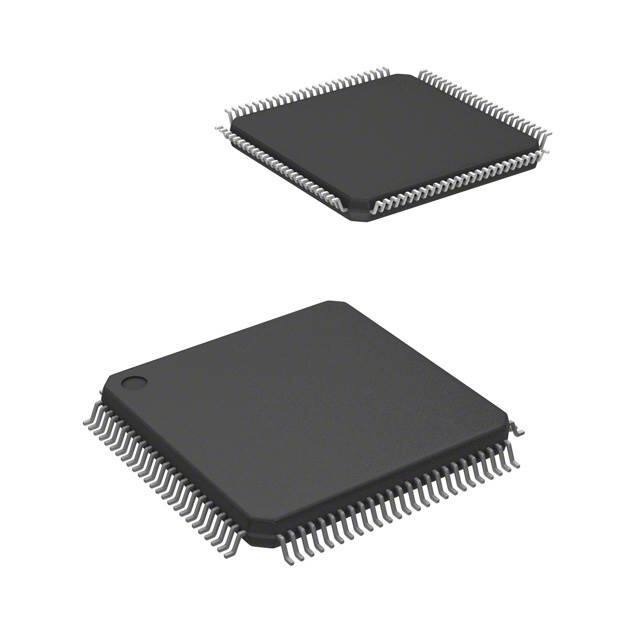


 工商网监
湘ICP备2023018690号
工商网监
湘ICP备2023018690号
